B
A
V99
BAV99, Rev.
B
Small Signal Diode
Absolute Maximum Ratings*
T
A
= 25∞C unless otherwise noted
*
These ratings are limiting values above which the serviceability of any semiconductor device may be impaired.
NOTES:
1) These ratings are based on a maximum junction temperature of 150 degrees C.
2) These are steady state limits. The factory should be consulted on applications involving pulsed or low duty cycle operations.
Thermal Characteristics
Symbol
Parameter
Value
Units
V
RRM
Maximum
Repetitive
Reverse
Voltage
70
V
I
F(AV)
Average
Rectified
Forward
Current
200
mA
I
FSM
Non-repetitive Peak Forward Surge Current
Pulse width = 1.0 second
Pulse width = 1.0 microsecond
1.0
2.0
A
A
T
stg
Storage Temperature Range
-55 to +150
∞
C
T
J
Operating
Junction
Temperature
150
∞
C
BAV99
SOT-23
3
1
2
2001 Fairchild Semiconductor Corporation
Symbol
Parameter
Test Conditions
Min
Max
Units
V
R
Breakdown
Voltage I
R
= 100
µ
A
70 V
V
F
Forward
Voltage
I
F
= 1.0 mA
I
F
= 10 mA
I
F
= 50 mA
I
F
= 150 mA
715
855
1.0
1.25
mV
mV
V
V
I
R
Reverse
Current
V
R
= 70 V
V
R
= 25 V, T
A
= 150
∞
C
V
R
= 70 V, T
A
= 150
∞
C
2.5
30
50
µ
A
µ
A
µ
A
C
T
Total
Capacitance
V
R
= 0, f
= 1.0 MHz
1.5
pF
t
rr
Reverse Recovery Time
I
F
= I
R
= 10 mA, I
RR
= 1.0 mA,
R
L
= 100
6.0 ns
Electrical Characteristics
T
A
= 25∞C unless otherwise noted
Symbol
Parameter
Value
Units
P
D
Power
Dissipation
350
mW
R
JA
Thermal Resistance, Junction to Ambient
357
∞
C/W
1
2
3
A7
1
2
3
Connection Diagram
B
A
V99
BAV99, Rev.
B
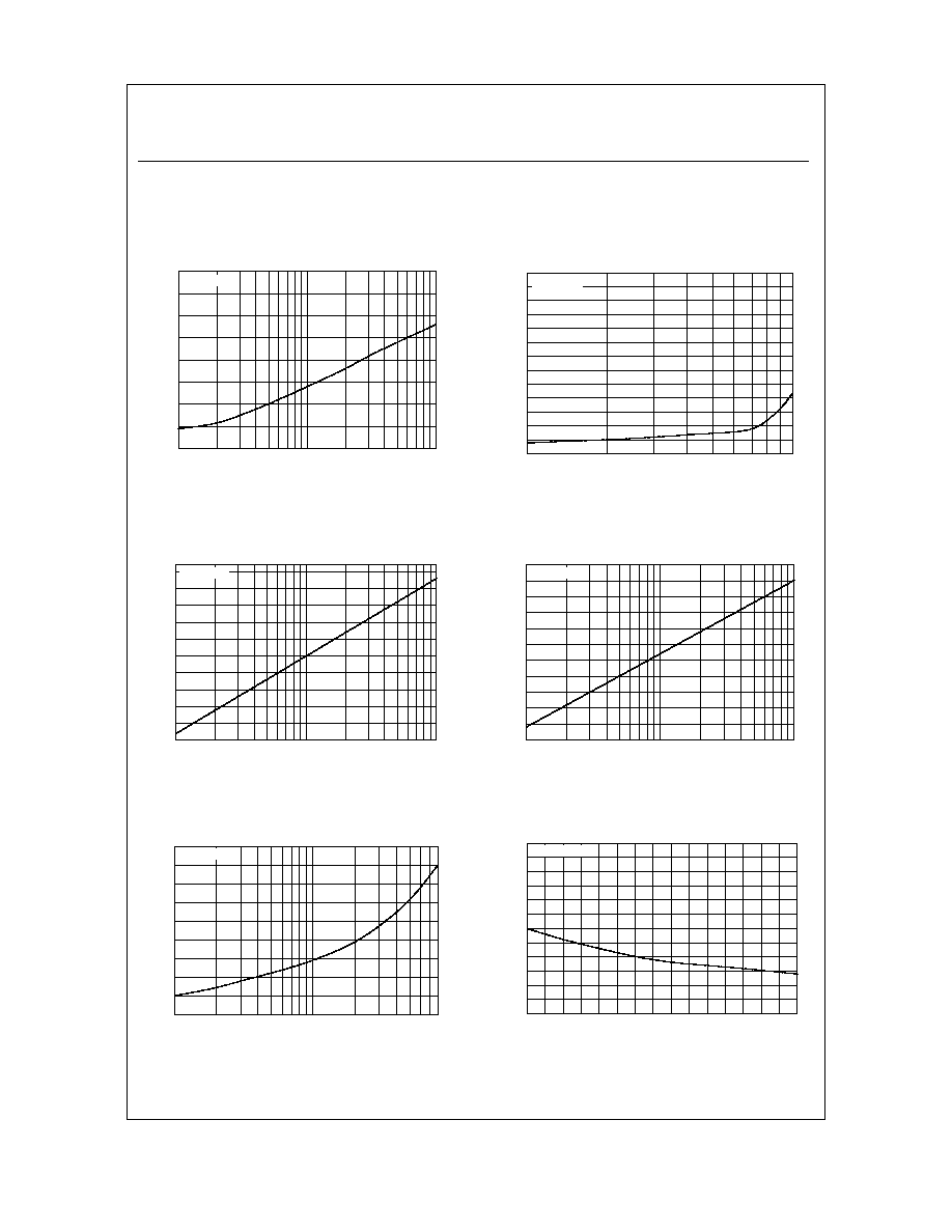
Typical Characteristics
Small Signal Diode
(continued)
110
120
130
140
150
1 2 3 5 10 20 30 50 100
Ta= 25 C
Rever
s
e Vol
t
age,
V
R
[V
]
Reverse Current, I
R
[uA]
0
50
100
150
200
250
300
10 20 30 50 70 100
Ta= 25 C
R
e
vers
e C
u
r
r
ent,
I
R
[n
A
]
Reverse Voltage, V
R
[V]
250
300
350
400
450
1 2 3 5 10 20 30 50 100
Ta= 25 C
F
o
rw
ard V
o
l
t
a
ge,
V
F
[m
V
]
Forward Current, I
F
[uA]
450
500
550
600
650
700
0.1 0.2 0.3 0.5 1 2 3 5 10
Ta= 25 C
Fo
r
w
a
r
d Vo
l
t
ag
e
,
V
F
[m
V
]
Forward Current, I
F
[mA]
0.6
0.8
1.0
1.2
1.4
10 20 30 50 100 200 300 500
Ta= 25 C
For
w
a
r
d Vol
t
age,
V
F
[V
]
Forw ard C urrent, I
F
[m A ]
0
2
4
6
8
10
12
14
1.0
1.1
1.2
1.3
Ta= 25 C
To
t
a
l
Capa
c
i
t
anc
e
[
p
F
]
Reverse V oltage [V]
Figure 1. Reverse Voltage vs Reverse Current
BV - 1.0 to 100uA
Figure 2. Reverse Current vs Reverse Voltage
IR - 10 to 100 V
Figure 3. Forward Voltage vs Forward Current
VF - 1.0 to 100 uA
Figure 4. Forward Voltage vs Forward Current
VF - 0.1 to 10 mA
Figure 5. Forward Voltage vs Forward Current
VF - 10 - 800 mA
Figure 6. Total Capacitance vs Reverse Voltage
∞
∞
∞
∞
∞
∞
DISCLAIMER
FAIRCHILD SEMICONDUCTOR RESERVES THE RIGHT TO MAKE CHANGES WITHOUT FURTHER
NOTICE TO ANY PRODUCTS HEREIN TO IMPROVE RELIABILITY, FUNCTION OR DESIGN. FAIRCHILD
DOES NOT ASSUME ANY LIABILITY ARISING OUT OF THE APPLICATION OR USE OF ANY PRODUCT
OR CIRCUIT DESCRIBED HEREIN; NEITHER DOES IT CONVEY ANY LICENSE UNDER ITS PATENT
RIGHTS, NOR THE RIGHTS OF OTHERS.
TRADEMARKS
The following are registered and unregistered trademarks Fairchild Semiconductor owns or is authorized to use and is
not intended to be an exhaustive list of all such trademarks.
LIFE SUPPORT POLICY
FAIRCHILD'S PRODUCTS ARE NOT AUTHORIZED FOR USE AS CRITICAL COMPONENTS IN LIFE SUPPORT
DEVICES OR SYSTEMS WITHOUT THE EXPRESS WRITTEN APPROVAL OF FAIRCHILD SEMICONDUCTOR CORPORATION.
As used herein:
1. Life support devices or systems are devices or
systems which, (a) are intended for surgical implant into
the body, or (b) support or sustain life, or (c) whose
failure to perform when properly used in accordance
with instructions for use provided in the labeling, can be
reasonably expected to result in significant injury to the
user.
2. A critical component is any component of a life
support device or system whose failure to perform can
be reasonably expected to cause the failure of the life
support device or system, or to affect its safety or
effectiveness.
PRODUCT STATUS DEFINITIONS
Definition of Terms
Datasheet Identification
Product Status
Definition
Advance Information
Preliminary
No Identification Needed
Obsolete
This datasheet contains the design specifications for
product development. Specifications may change in
any manner without notice.
This datasheet contains preliminary data, and
supplementary data will be published at a later date.
Fairchild Semiconductor reserves the right to make
changes at any time without notice in order to improve
design.
This datasheet contains final specifications. Fairchild
Semiconductor reserves the right to make changes at
any time without notice in order to improve design.
This datasheet contains specifications on a product
that has been discontinued by Fairchild semiconductor.
The datasheet is printed for reference information only.
Formative or
In Design
First Production
Full Production
Not In Production
OPTOLOGICTM
OPTOPLANARTM
PACMANTM
POPTM
Power247TM
PowerTrench
QFETTM
QSTM
QT OptoelectronicsTM
Quiet SeriesTM
SILENT SWITCHER
FAST
FASTrTM
FRFETTM
GlobalOptoisolatorTM
GTOTM
HiSeCTM
ISOPLANARTM
LittleFETTM
MicroFETTM
MicroPakTM
MICROWIRETM
Rev. H4
Æ
ACExTM
BottomlessTM
CoolFETTM
CROSSVOLT
TM
DenseTrenchTM
DOMETM
EcoSPARKTM
E
2
CMOS
TM
EnSigna
TM
FACTTM
FACT Quiet SeriesTM
SMART STARTTM
STAR*POWERTM
StealthTM
SuperSOTTM-3
SuperSOTTM-6
SuperSOTTM-8
SyncFETTM
TinyLogicTM
TruTranslationTM
UHCTM
UltraFET
Æ
Æ
Æ
STAR*POWER is used under license
VCXTM