 | ÐлекÑÑоннÑй компоненÑ: BCW65C | СкаÑаÑÑ:  PDF PDF  ZIP ZIP |
Äîêóìåíòàöèÿ è îïèñàíèÿ www.docs.chipfind.ru
BCW65C
BCW65C
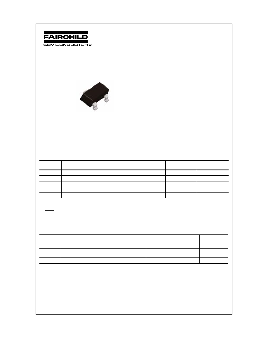
NPN General Purpose Amplifier
This device is designed for general purpose amplifier applications
at collector currents to 500 mA. Sourced from Process 19.
C
E
B
SOT-23
Mark: ED
Absolute Maximum Ratings*
TA = 25°C unless otherwise noted
*
These ratings are limiting values above which the serviceability of any semiconductor device may be impaired.
NOTES:
1) These ratings are based on a maximum junction temperature of 150 degrees C.
2) These are steady state limits. The factory should be consulted on applications involving pulsed or low duty cycle operations.
Thermal Characteristics
TA = 25°C unless otherwise noted
Symbol
Parameter
Value
Units
V
CEO
Collector-Emitter Voltage
32
V
V
CBO
Collector-Base Voltage
60
V
V
EBO
Emitter-Base Voltage
5.0
V
I
C
Collector Current - Continuous
1.0
A
T
J
, T
stg
Operating and Storage Junction Temperature Range
-55 to +150
°
C
Symbol
Characteristic
Max
Units
*BCW65C
P
D
Total Device Dissipation
Derate above 25
°
C
350
2.8
mW
mW/
°
C
R
JA
Thermal Resistance, Junction to Ambient
357
°
C/W
*
Device mounted on FR-4 PCB 40 mm X 40 mm X 1.5 mm.
Discrete POWER & Signal
Technologies
ã
1997 Fairchild Semiconductor Corporation
BCW65C
OFF CHARACTERISTICS
V
(BR)CEO
Collector-Emitter Breakdown Voltage
I
C
= 10 mA, I
B
= 0
32
V
V
(BR)CBO
Collector-Base Breakdown Voltage
I
C
= 10
µ
A, I
E
= 0
60
V
V
(BR)EBO
Emitter-Base Breakdown Voltage
I
E
= 10
µ
A, I
C
= 0
5.0
V
I
CES
Collector-Cutoff Current
V
CB
= 32 V, I
E
= 0
V
CB
= 32 V, I
E
= 0, T
A
= 150
°
C
20
20
nA
µ
A
I
EBO
Emitter-Cutoff Current
V
EB
= 4.0 V, I
C
= 0
20
nA
Electrical Characteristics
TA = 25°C unless otherwise noted
Symbol
Parameter
Test Conditions
Min
Max
Units
ON CHARACTERISTICS
h
FE
DC Current Gain
I
C
= 100
µ
A, V
CE
= 10 V
I
C
= 10 mA, V
CE
= 1.0 V
I
C
= 100 mA, V
CE
= 1.0 V
I
C
= 500 mA, V
CE
= 2.0 V
80
180
250
50
630
V
CE(
sat
)
Collector-Emitter Saturation Voltage
I
C
= 100 mA, I
B
= 10 mA
I
C
= 500 mA,
B
= 50 mA
0.3
0.7
V
V
BE(
sat
)
Base-Emitter Saturation Voltage
I
C
= 500 mA, I
B
= 50 mA
2.0
V
SMALL SIGNAL CHARACTERISTICS
f
T
Current Gain - Bandwidth Product
I
C
= 20 mA, V
CE
= 10 V,
f = 100 MHz
100
MHz
C
obo
Output Capacitance
V
CB
= 10 V, I
E
= 0, f = 1.0 MHz
12
pF
C
ibo
Input Capacitance
V
EB
= 0.5 V, I
C
= 0, f = 1.0 MHz
80
pF
NF
Noise Figure
I
C
= 0.2 mA, V
CE
= 5.0,
R
S
= 1.0 k
, f = 1.0 kHz,
BW = 200 Hz
10
dB
NPN General Purpose Amplifier
(continued)
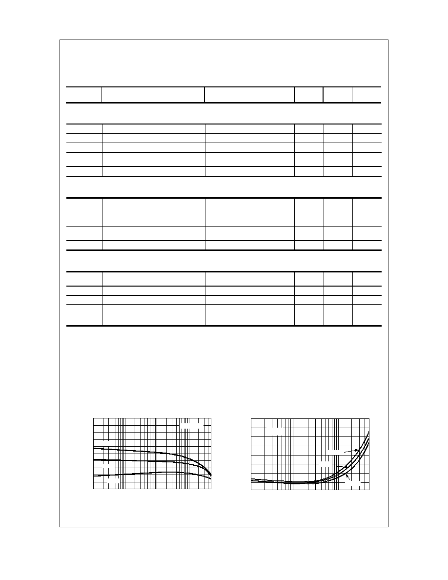
Typical Characteristics
Collector-Emitter Saturation
Voltage vs Collector Current
1
10
100
500
0.1
0.2
0.3
0.4
I - COLLECTOR CURRENT (mA)
V
-
COLL
ECT
O
R
-
EMI
T
TER VOL
T
A
G
E
(
V
)
CES
A
T
25 °C
C
= 10
125 °C
- 40 °C
Typical Pulsed Current Gain
vs Collector Current
0.1
0.3
1
3
10
30
100
300
0
100
200
300
400
500
I - COLLECTOR CURRENT (mA)
h
-
TYPI
C
A
L P
U
LS
ED CU
RRENT
GA
I
N
C
FE
125 °C
25 °C
- 40 °C
V = 5V
CE
BCW65C
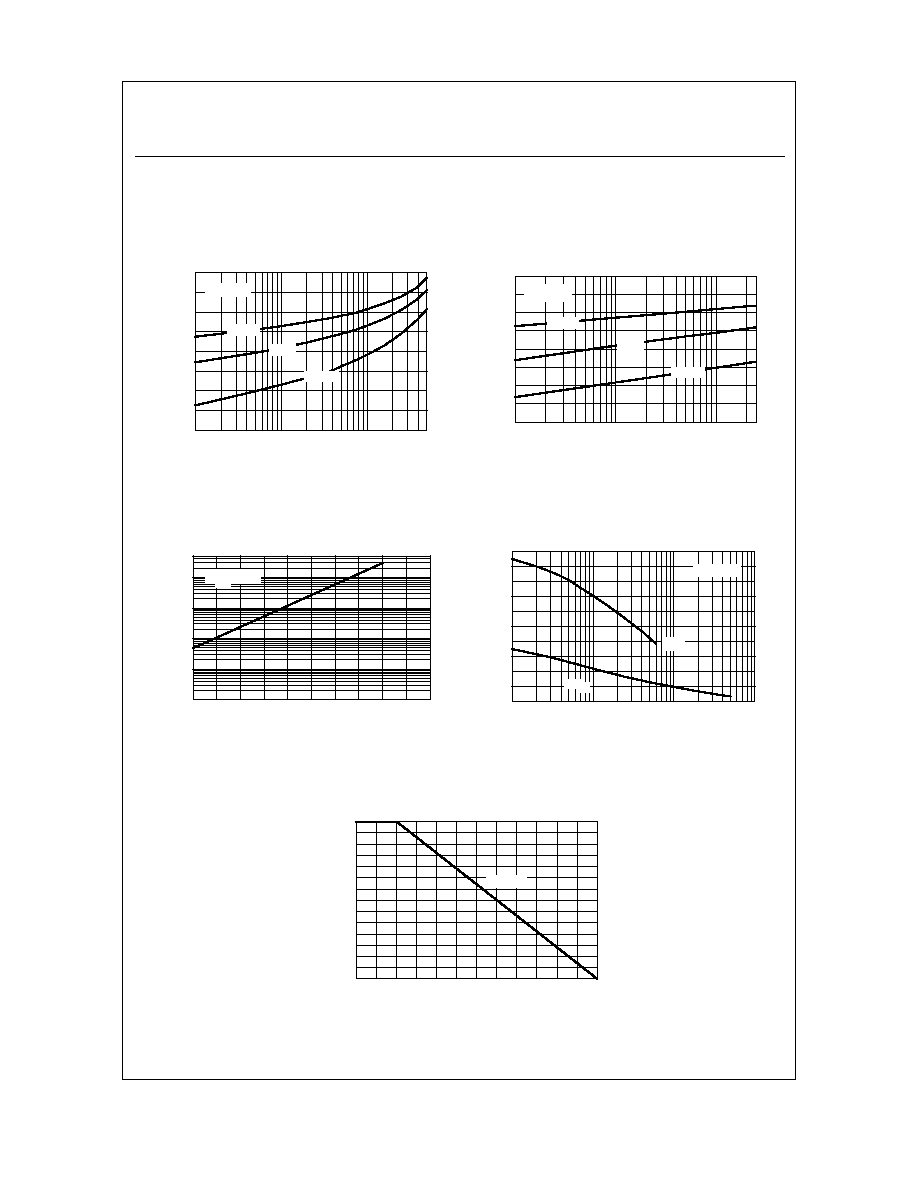
NPN General Purpose Amplifier
(continued)
Typical Characteristics
Base-Emitter ON Voltage vs
Collector Current
0.1
1
10
25
0.2
0.4
0.6
0.8
1
I - COLLECTOR CURRENT (mA)
V
-
B
A
SE-
EM
I
T
T
E
R
ON VOL
T
A
G
E (
V
)
BE
(
O
N
)
C
V = 5V
CE
25 °C
125 °C
- 40 °C
Base-Emitter Saturation
Voltage vs Collector Current
1
10
100
500
0.4
0.6
0.8
1
I - COLLECTOR CURRENT (mA)
V
- BA
SE-EM
I
TTER
VO
L
T
A
G
E
(V)
BE
SA
T
C
= 10
25 °C
125 °C
- 40 °C
Collector-Cutoff Current
vs Ambient Temperature
25
50
75
100
125
150
0.1
1
10
100
500
T - AMBIENT TEMPERATURE ( C)
I
- COLL
ECT
O
R
CURRE
NT (nA
)
A
V
= 40V
CB
CB
O
°
Emitter Transition and Output
Capacitance vs Reverse Bias Voltage
0.1
1
10
100
4
8
12
16
20
REVERSE BIAS VOLTAGE (V)
CA
P
A
CI
T
A
N
C
E (
p
F
)
f = 1 MHz
C ob
C te
Power Dissipation vs
Ambient Temperature
0
25
50
75
100
125
150
0
50
100
150
200
250
300
350
TEMPERATURE ( C)
P
-
POW
E
R DISSI
P
A
TI
ON (
m
W
)
D
o
SOT-23
TRADEMARKS
ACExTM
CoolFETTM
CROSSVOLTTM
E
2
CMOS
TM
FACTTM
FACT Quiet SeriesTM
FAST
®
FASTrTM
GTOTM
HiSeCTM
The following are registered and unregistered trademarks Fairchild Semiconductor owns or is authorized to use and is
not intended to be an exhaustive list of all such trademarks.
LIFE SUPPORT POLICY
FAIRCHILD'S PRODUCTS ARE NOT AUTHORIZED FOR USE AS CRITICAL COMPONENTS IN LIFE SUPPORT
DEVICES OR SYSTEMS WITHOUT THE EXPRESS WRITTEN APPROVAL OF FAIRCHILD SEMICONDUCTOR CORPORATION.
As used herein:
ISOPLANARTM
MICROWIRETM
POPTM
PowerTrenchTM
QSTM
Quiet SeriesTM
SuperSOTTM-3
SuperSOTTM-6
SuperSOTTM-8
TinyLogicTM
1. Life support devices or systems are devices or
systems which, (a) are intended for surgical implant into
the body, or (b) support or sustain life, or (c) whose
failure to perform when properly used in accordance
with instructions for use provided in the labeling, can be
reasonably expected to result in significant injury to the
user.
2. A critical component is any component of a life
support device or system whose failure to perform can
be reasonably expected to cause the failure of the life
support device or system, or to affect its safety or
effectiveness.
PRODUCT STATUS DEFINITIONS
Definition of Terms
Datasheet Identification Product Status Definition
Advance Information
Preliminary
No Identification Needed
Obsolete
This datasheet contains the design specifications for
product development. Specifications may change in
any manner without notice.
This datasheet contains preliminary data, and
supplementary data will be published at a later date.
Fairchild Semiconductor reserves the right to make
changes at any time without notice in order to improve
design.
This datasheet contains final specifications. Fairchild
Semiconductor reserves the right to make changes at
any time without notice in order to improve design.
This datasheet contains specifications on a product
that has been discontinued by Fairchild semiconductor.
The datasheet is printed for reference information only.
Formative or
In Design
First Production
Full Production
Not In Production
DISCLAIMER
FAIRCHILD SEMICONDUCTOR RESERVES THE RIGHT TO MAKE CHANGES WITHOUT FURTHER
NOTICE TO ANY PRODUCTS HEREIN TO IMPROVE RELIABILITY, FUNCTION OR DESIGN. FAIRCHILD
DOES NOT ASSUME ANY LIABILITY ARISING OUT OF THE APPLICATION OR USE OF ANY PRODUCT
OR CIRCUIT DESCRIBED HEREIN; NEITHER DOES IT CONVEY ANY LICENSE UNDER ITS PATENT
RIGHTS, NOR THE RIGHTS OF OTHERS.