October 1987
Revised January 1999
CD401
4BC
8-
S
t
a
g
e Stat
ic Shi
f
t
Regi
ster
© 1999 Fairchild Semiconductor Corporation
DS005947.prf
www.fairchildsemi.com
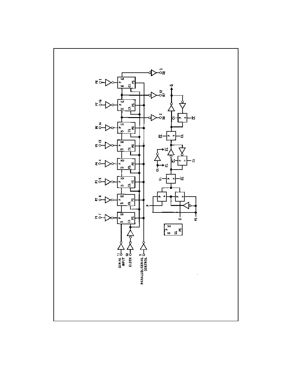
CD4014BC
8-Stage Static Shift Register
General Description
The CD4014BC is an 8-stage parallel input/serial output
shift register. A parallel/serial control input enables individ-
ual JAM inputs to each of 8 stages. Q outputs are available
from the sixth, seventh and eighth stages. All outputs have
equal source and sink current capabilities and conform to
standard "B" series output drive.
When the parallel/serial control input is in the logical "0"
state, data is serially shifted into the register synchronously
with the positive transition of the clock. When the parallel/
serial control input is in the logical "1" state, data is jammed
into each stage of the register synchronously with the posi-
tive transition of the clock.
All inputs are protected against static discharge with diodes
to V
DD
and V
SS
.
Features
s
Wide supply voltage range:
3.0V to 15V
s
High noise immunity:
0.45 V
DD
(typ.)
s
Low power TTL compatibility:
Fan out of 2 driving 74L
or 1 driving 74LS
s
5V≠10V≠15V parametric ratings
s
Symmetrical output characteristics
s
Maximum input leakage:
1
µ
A at 15V over full temperature range
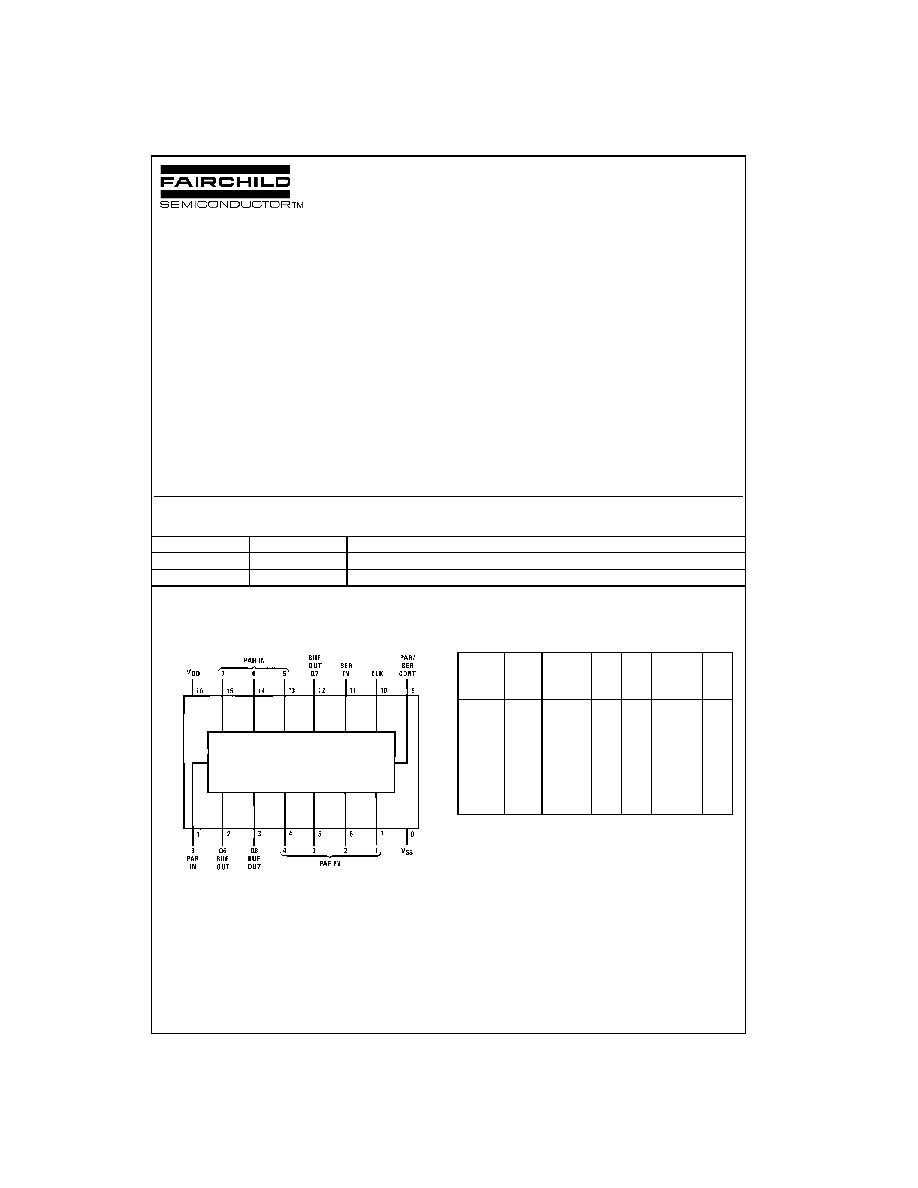
Ordering Code:
Devices also available in Tape and Reel. Specify by appending the suffix letter "x" to the ordering code.
Connection Diagram
Pin Assignments for DIP
Top View
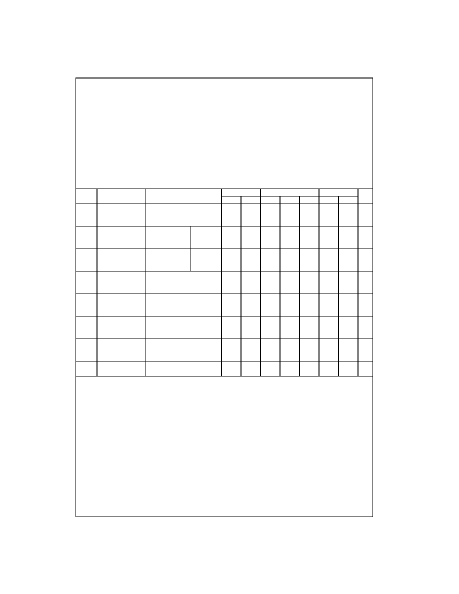
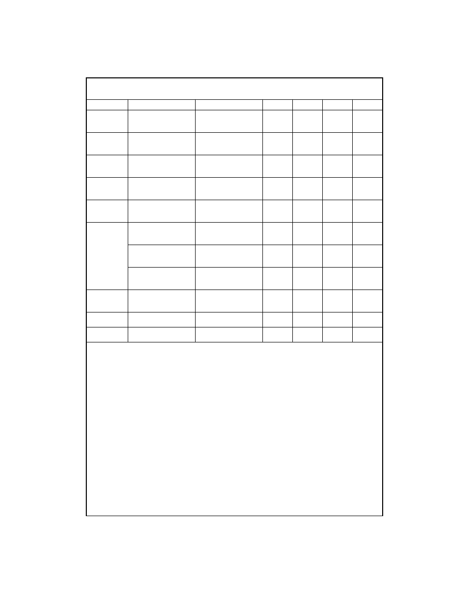
Truth Table
X
=
Don't care case
No Change
Note 1: Level change
Order Number
Package Number
Package Description
CD4014BCM
M16A
16-Lead Small Outline Integrated Circuit (SOIC), JEDEC MS-012, 0.150" Narrow
CD4014BCN
N16E
16-Lead Plastic Dual-In-Line Package (PDIP), JEDEC MS-100, 0.300" Wide
CL
(Note 1)
Serial
Input
Parallel/
Serial
Control
PI 1
PI n
Q1
(Internal)
Q
n
X
1
0
0
0
0
X
1
1
0
1
0
X
1
0
1
0
1
X
1
1
1
1
1
0
0
X
X
0
Q
n
-
1
1
0
X
X
1
Q
n
-
1
X
X
X
X
Q1
Q
n
3
www.fairchildsemi.com
CD401
4BC
Absolute Maximum Ratings
(Note 2)
(Note 3)
Recommended Operating
Conditions
(Note 3)
Note 2: "Absolute Maximum Ratings" are those values beyond which the
safety of the device cannot be guaranteed. Except for "Operating Tempera-
ture Range" they are not meant to imply that the devices should be oper-
ated at these limits. The table of "Electrical Characteristics" provides
conditions for actual device operation.
Note 3: V
SS
=
0V unless otherwise specified.
DC Electrical Characteristics
(Note 3)
Note 4: I
OL
and I
OH
are tested one output at a time.
Supply Voltage (V
DD
)
-
0.5V to
+
18V
Input Voltage (V
IN
)
-
0.5 to V
DD
+
0.5V
Storage Temperature Range (T
S
)
-
65
∞
C to
+
150
∞
C
Power Dissipation (P
D
)
Dual-In-Line
700 mW
Small Outline
500 mW
Lead Temperature (T
L
)
(Soldering, 10 seconds)
260
∞
C
Supply Voltage (V
DD
)
3.0V to 15V
Input Voltage (V
IN
)
0 to V
DD
Operating Temperature Range (T
A
)
-
40
∞
C to
+
85
∞
C
Symbol
Parameter
Conditions
-
40
∞
C
+
25
∞
C
+
85
∞
C
Units
Min
Max
Min
Typ
Max
Min
Max
I
DD
Quiescent Device
V
DD
=
5V, V
IN
=
V
DD
or V
SS
20
0.1
20
150
µ
A
Current
V
DD
=
10V, V
IN
=
V
DD
or V
SS
40
0.2
40
300
µ
A
V
DD
=
15V, V
IN
=
V
DD
or V
SS
80
0.3
80
600
µ
A
V
OL
LOW Level
V
DD
=
5V
0.05
0
0.05
0.05
V
Output Voltage
V
DD
=
10V
|I
O
|
<
1
µ
A
0.05
0
0.05
0.05
V
V
DD
=
15V
0.05
0
0.05
0.05
V
V
OH
HIGH Level
V
DD
=
5V
4.95
4.95
5
4.95
V
Output Voltage
V
DD
=
10V
|I
O
|
<
1
µ
A
9.95
9.95
10
9.95
V
V
DD
=
15V
14.95
14.95
15
14.95
V
V
IL
LOW Level
V
DD
=
5V, V
O
=
0.5V or 4.5V
1.5
2
1.5
1.5
V
Input Voltage
V
DD
=
10V, V
O
=
1.0V or 9.0V
3.0
4
3.0
3.0
V
V
DD
=
15V, V
O
=
1.5V or 13.5V
4.0
6
4.0
4.0
V
V
IH
HIGH Level
V
DD
=
5V, V
O
=
0.5V or 4.5V
3.5
3.5
3
3.5
V
Input Voltage
V
DD
=
10V, V
O
=
1.0V or 9.0V
7.0
7.0
6
7.0
V
V
DD
=
15V, V
O
=
1.5V or 13.5V
11.0
11.0
9
11.0
V
I
OL
LOW Level Output
V
DD
=
5V, V
O
=
0.4V
0.52
0.44
0.88
0.36
mA
Current (Note 4)
V
DD
=
10V, V
O
=
0.5V
1.3
1.1
2.2
0.9
mA
V
DD
=
15V, V
O
=
1.5V
3.6
3.0
8
2.4
mA
I
OH
HIGH Level Output
V
DD
=
5V, V
O
=
4.6V
-
0.52
-
0.44
-
0.88
-
0.36
mA
Current (Note 4)
V
DD
=
10V, V
O
=
9.5V
-
1.3
-
1.1
-
2.2
-
0.90
mA
V
DD
=
15V, V
O
=
13.5V
-
3.6
-
3.0
-
8
-
2.4
mA
I
IN
Input Current
V
DD
=
15V, V
IN
=
0V
-
0.3
-
10
-
5
-
0.3
-
1.0
µ
A
V
DD
=
15V, V
IN
=
15V
0.3
10
-
5
0.3
1.0
µ
A
www.fairchildsemi.com
4
C
D
40
14BC
AC Electrical Characteristics
(Note 5)
T
A
=
25
∞
C, input t
r
, t
f
=
20 ns, C
L
=
50 pF, R
L
=
200 k
Note 5: AC Parameters are guaranteed by DC correlated testing.
Note 6: If more than one unit is cascaded t
rCL
should be made less than or equal to the fixed propagation delay of the output of the driving stage for the esti-
mated capacitive load.
Note 7: Setup times are measured with reference to clock and a fixed hold time (t
H
) as specified.
Note 8: C
PD
determines the no load AC power consumption of any CMOS device. For complete explanation, see 74C family characteristics application note
AN-90.
Symbol
Parameter
Conditions
Min
Typ
Max
Units
t
PHL
, t
PLH
Propagation Delay Time
V
DD
=
5V
200
320
ns
V
DD
=
10V
80
160
ns
V
DD
=
15V
60
120
ns
t
THL
, t
TLH
Transition Time
V
DD
=
5V
100
200
ns
V
DD
=
10V
50
100
ns
V
DD
=
15V
40
80
ns
f
CL
Maximum Clock
V
DD
=
5V
2.8
4
MHz
Input Frequency
V
DD
=
10V
6
12
MHz
V
DD
=
15V
8
16
MHz
t
W
Minimum Clock
V
DD
=
5V
90
180
ns
Pulse Width
V
DD
=
10V
40
80
ns
V
DD
=
15V
25
50
ns
t
rCL
, t
fCL
Clock Rise and
V
DD
=
5V
15
µ
s
Fall Time (Note 6)
V
DD
=
10V
15
µ
s
V
DD
=
15V
15
µ
s
t
S
Minimum Set-Up Time
V
DD
=
5V
60
120
ns
(Note 7) Serial Input
V
DD
=
10V
40
80
ns
t
H
200 ns
V
DD
=
15V
30
60
ns
Parallel Inputs
V
DD
=
5V
80
160
ns
t
H
200 ns
V
DD
=
10V
40
80
ns
V
DD
=
15V
30
60
ns
Parallel/Serial Control
V
DD
=
5V
100
200
ns
t
H
200 ns
V
DD
=
10V
50
100
ns
V
DD
=
15V
40
80
ns
t
H
Minimum Hold Time
V
DD
=
5V
0
ns
Serial In, Parallel In, t
S
400 ns V
DD
=
10V
10
ns
Parallel/Serial Control
V
DD
=
15V
15
ns
C
I
Average Input Capacitance
Any Input
5
7.5
pF
(Note 8)
C
PD
Power Dissipation Capacitance
110
pF
(Note 8)