© 2002 Fairchild Semiconductor Corporation
DS005959
www.fairchildsemi.com
October 1987
Revised March 2002
CD402
8BC
BCD-t
o
-Deci
m
a
l Decoder
CD4028BC
BCD-to-Decimal Decoder
General Description
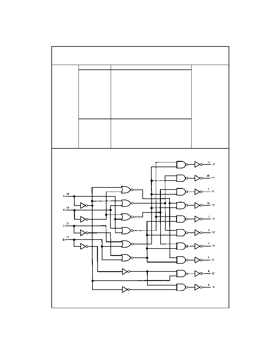
The CD4028BC is a BCD-to-decimal or binary-to-octal
decoder consisting of 4 inputs, decoding logic gates, and
10 output buffers. A BCD code applied to the 4 inputs, A, B,
C, and D, results in a high level at the selected 1-of-10 dec-
imal decoded outputs. Similarly, a 3-bit binary code applied
to inputs A, B, and C is decoded in octal at outputs 0≠7. A
high level signal at the D input inhibits octal decoding and
causes outputs 0≠7 to go LOW.
All inputs are protected against static discharge damage by
diode clamps to V
DD
and V
SS
.
Features
s
Wide supply voltage range:
3.0V to 15V
s
High noise immunity:
0.45 V
DD
(typ.)
s
Low power TTL compatibility:
fan out of 2 driving 74L
or 1 driving 74LS
s
Low power
s
Glitch free outputs
s
"Positive logic" on inputs and outputs
Applications
∑ Code conversion
∑ Address decoding
∑ Indicator-tube decoder
Ordering Code:
Devices also available in Tape and Reel. Specify by appending the suffix letter "X" to the ordering code.
Connection Diagram
Top View
Order Number
Package Number
Package Description
CD4028BCM
M16A
16-Lead Small Outline Integrated Circuit (SOIC), JEDEC MS-012, 0.150" Narrow
CD4028BCN
N16E
16-Lead Plastic Dual-In-Line Package (PDIP), JEDEC MS-001, 0.300" Wide

3
www.fairchildsemi.com
CD402
8BC
Absolute Maximum Ratings
(Note 1)
(Note 2)
Recommended Operating
Conditions
(Note 2)
Note 1: "Absolute Maximum Ratings" are those values beyond which the
safety of the device cannot be guaranteed, they are not meant to imply that
the devices should be operated at these limits. The table of "Recom-
mended Operating Conditions" and "Electrical Characteristics" provides
conditions for actual device operation.
Note 2: V
SS
=
0V unless otherwise specified.
DC Electrical Characteristics
(Note 2)
Note 3: I
OL
and I
OH
are tested one output at a time.
Supply Voltage (V
DD
)
-
0.5 to
+
18V
Input Voltage (V
IN
)
-
0.5 to V
DD
+
0.5V
Storage Temperature Range (T
S
)
-
65
∞
C to
+
150
∞
C
Power Dissipation (P
D
)
Dual-In-Line
700 mW
Small Outline
500 mW
Lead Temperature (T
L
)
(Soldering, 10 seconds)
260
∞
C
Supply Voltage (V
DD
)
3 to 15V
Input Voltage (V
IN
)
0 to V
DD
V
Operating Temperature Range (T
A
)
-
55
∞
C to
+
125
∞
C
Symbol
Parameter
Conditions
-
55
∞
C
+
25
∞
C
+
125
∞
C
Units
Min
Max
Min
Typ
Max
Min
Max
I
DD
Quiescent Device Current
V
DD
=
5V,
V
IN
=
V
DD
or V
SS
5
0.01
5
150
µ
A
V
DD
=
10V, V
IN
=
V
DD
or V
SS
10
0.01
10
300
V
DD
=
15V, V
IN
=
V
DD
or V
SS
20
0.02
20
600
V
OL
LOW Level Output Voltage
|I
O
|
<
1
µ
A, V
IL
=
0V, V
IH
=
V
DD
V
DD
=
5V
0.05
0
0.05
0.05
V
V
DD
=
10V
0.05
0
0.05
0.05
V
DD
=
15V
0.05
0
0.05
0.05
V
OH
HIGH Level Output Voltage
|I
O
|
<
1
µ
A, V
IL
=
0V, V
IH
=
V
DD
V
DD
=
5V
4.95
4.95
5
4.95
V
V
DD
=
10V
9.95
9.95
10
9.95
V
DD
=
15V
14.95
14.95
15
14.95
V
IL
LOW Level Input Voltage
|I
O
|
<
1
µ
A
V
DD
=
5V,
V
O
=
0.5V or 4.5V
1.5
2.25
1.5
1.5
V
V
DD
=
10V,
V
O
=
1V or 9V
3.0
4.5
3.0
3.0
V
DD
=
15V,
V
O
=
1.5V or 13.5V
4.0
6.75
4.0
4.0
V
IH
HIGH Level Input Voltage
|I
O
|
<
1
µ
A
V
DD
=
5V,
V
O
=
0.5V or 4.5V
3.5
3.5
2.75
3.5
V
V
DD
=
10V,
V
O
=
1V or 9V
7.0
7.0
5.5
7.0
V
DD
=
15V,
V
O
=
1.5V or 13.5V
11.0
11.0
8.25
11.0
I
OL
LOW Level Output Current
V
IH
=
V
DD
, V
IL
=
0V
(Note 3)
V
DD
=
5V,
V
O
=
0.4V
0.64
0.51
1.0
0.36
mA
V
DD
=
10V,
V
O
=
0.5V
1.6
1.3
2.6
0.9
V
DD
=
15V,
V
O
=
1.5V
4.2
3.4
6.8
2.4
I
OH
HIGH Level Output Current
V
IH
=
V
DD
, V
IL
=
0V
(Note 3)
V
DD
=
5V,
V
O
=
4.6V
-
0.25
-
0.2
-
0.4
-
0.14
mA
V
DD
=
10V,
V
O
=
9.5V
-
0.62
-
0.5
-
1.0
-
0.35
V
DD
=
15V,
V
O
=
13.5V
-
1.8
-
1.5
-
3.0
-
1.1
I
IN
Input Current
V
DD
=
15V,
V
IN
=
0V
-
0.1
-
0.1
-
1.0
µ
A
V
DD
=
15V,
V
IN
=
15V
0.1
0.1
1.0

www.fairchildsemi.com
4
C
D
40
28BC
AC Electrical Characteristics
(Note 4)
T
A
=
25
∞
C, C
L
=
50 pF, R
L
=
200k, Input t
r
=
t
f
=
20 ns, unless otherwise specified
Note 4: AC Parameters are guaranteed by DC correlated testing.
Switching Time Waveforms
Symbol
Parameter
Conditions
Min
Typ
Max
Units
t
PHL
or t
PLH
Propagation Delay Time
V
CC
=
5V
240
480
ns
V
CC
=
10V
100
200
V
CC
=
15V
70
140
t
THL
or t
TLH
Transition Time
V
CC
=
5V
175
350
ns
V
CC
=
10V
75
150
V
CC
=
15V
60
110
C
IN
Input Capacitance
Any Input
5
7.5
pF

5
www.fairchildsemi.com
CD402
8BC
Physical Dimensions
inches (millimeters) unless otherwise noted
16-Lead Small Outline Integrated Circuit (SOIC), JEDEC MS-012, 0.150" Narrow
Package Number M16A