October 1987
Revised January 1999
CD409
4BC
8-
B
i
t
Shi
f
t
Regi
ster
/La
t
c
h
w
i
t
h
3-
ST
A
T
E O
u
t
put
s
© 1999 Fairchild Semiconductor Corporation
DS005983.prf
www.fairchildsemi.com
CD4094BC
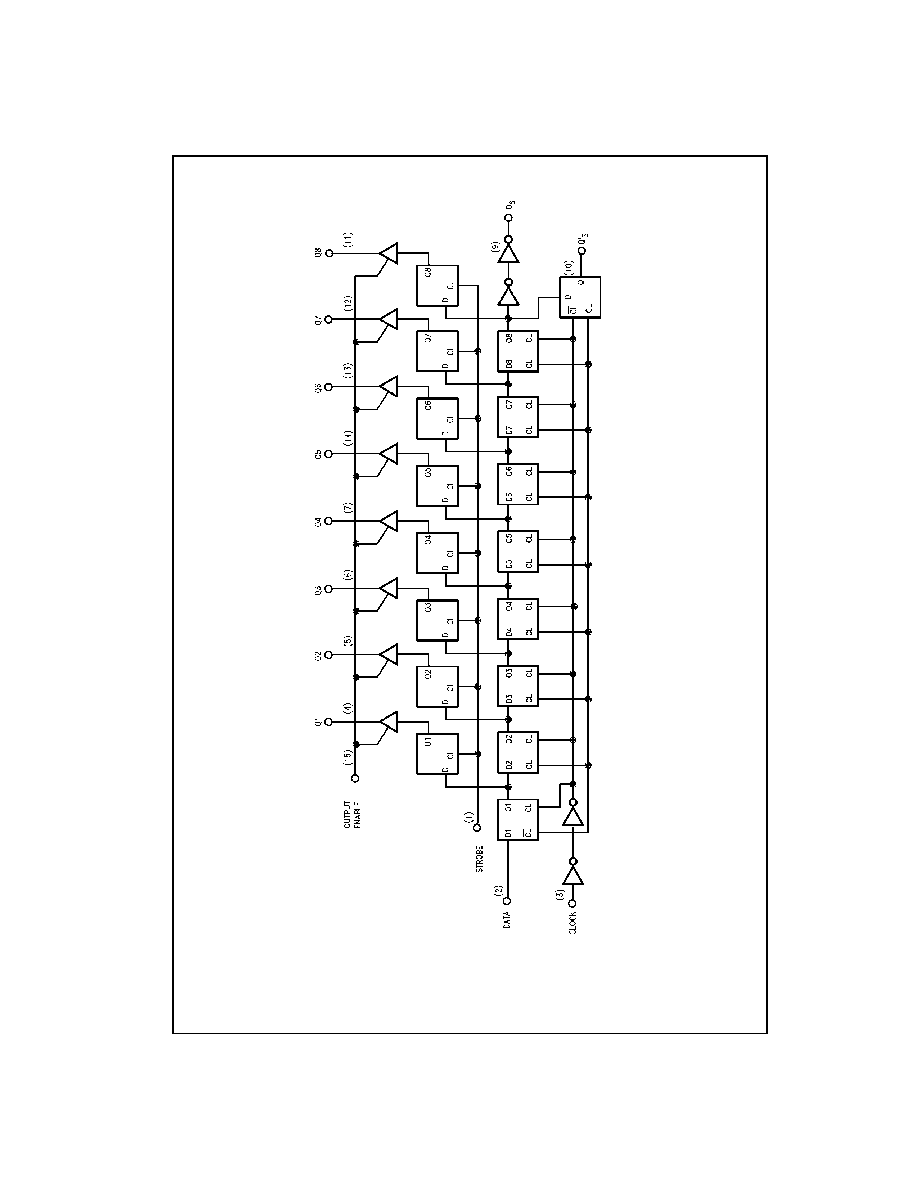
8-Bit Shift Register/Latch with 3-STATE Outputs
General Description
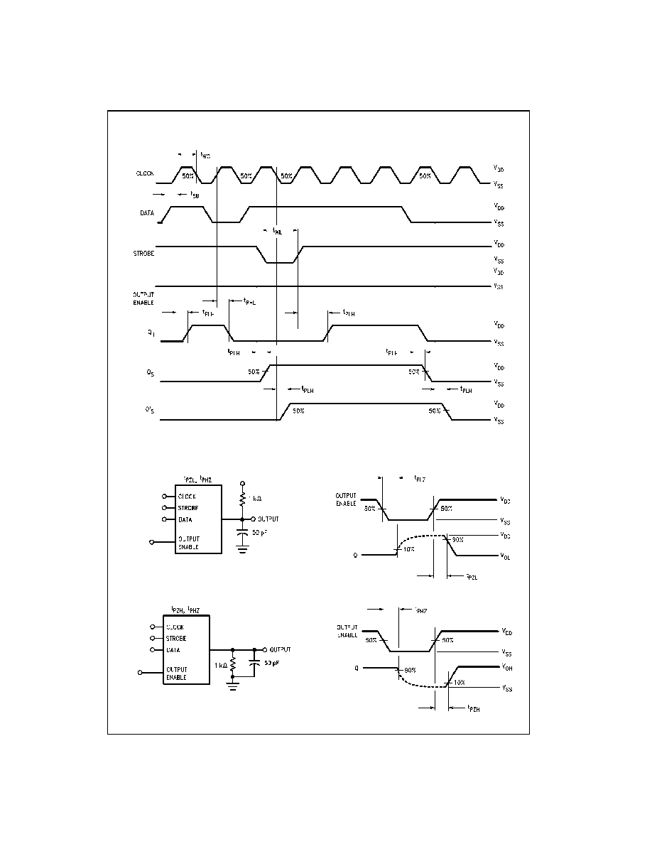
The CD4094BC consists of an 8-bit shift register and a 3-
STATE 8-bit latch. Data is shifted serially through the shift
register on the positive transition of the clock. The output of
the last stage (Q
S
) can be used to cascade several
devices. Data on the Q
S
output is transferred to a second
output, Q
S
, on the following negative clock edge.
The output of each stage of the shift register feeds a latch,
which latches data on the negative edge of the STROBE
input. When STROBE is HIGH, data propagates through
the latch to 3-STATE output gates. These gates are
enabled when OUTPUT ENABLE is taken HIGH.
Features
s
Wide supply voltage range:
3.0V to 18V
s
High noise immunity:
0.45 V
DD
(typ.)
s
Low power TTL compatibility:
Fan out of 2 driving 74L or 1 driving 74LS
s
3-STATE outputs
Ordering Code:
Devices also available in Tape and Reel. Specify by appending the suffix letter "X" to the ordering code.
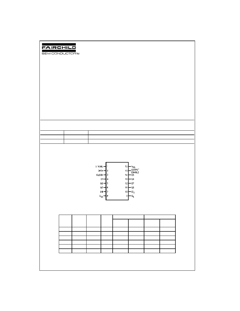
Connection Diagram
Pin Assignments for DIP and SOIC
Top View
Truth Table
X
=
Don't Care
=
HIGH-to-LOW
=
LOW-to-HIGH
Note 1: At the positive clock edge, information in the 7th shift register stage is transferred to Q8 and Q
S
.
Order Number
Package Number
Package Description
CD4094BCWM
M16B
16-Lead Small Outline Integrated Circuit (SOIC), JEDEC MS-013, 0.300" Wide
CD4094BCN
N16E
16-Lead Plastic Dual-In-Line Package (PDIP), JEDEC MS-001, 0.300" Wide
Clock
Output
Strobe
Data
Parallel Outputs
Serial Outputs
Enable
Q1
Q
N
Q
S
(Note 1)
Q
0
X
X
Hi-Z
Hi-Z
Q7
No Change
0
X
X
Hi-Z
Hi-Z
No Change
Q7
1
0
X
No Change No Change
Q7
No Change
1
1
0
0
Q
N
-
1
Q7
No Change
1
1
1
1
Q
N
-
1
Q7
No Change
1
1
1
No Change No Change No Change
Q7
3
www.fairchildsemi.com
CD409
4BC
Absolute Maximum Ratings
(Note 2)
(Note 3)
Recommended Operating
Conditions
(Note 3)
Note 2: "Absolute Maximum Ratings" are those values beyond which the
safety of the device cannot be guaranteed; they are not meant to imply that
the devices should be operated at these limits. The tables of "Recom-
mended Operating Conditions" and "Electrical Characteristics" provide con-
ditions for actual device operation.
Note 3: V
SS
=
0V unless otherwise specified.
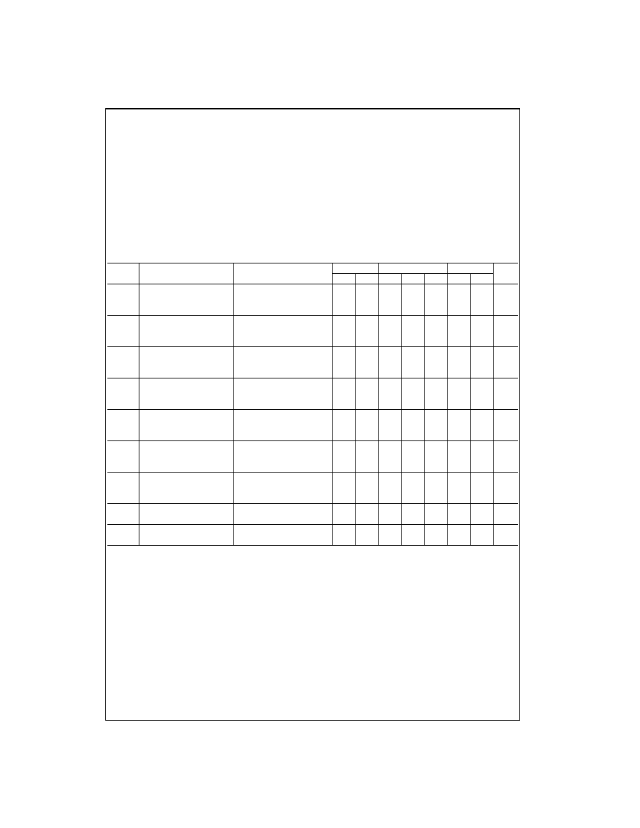
DC Electrical Characteristics
(Note 3)
Note 4: I
OH
and I
OL
are tested one output at a time.
Supply Voltage (V
DD
)
-
0.5 to
+
18 V
DC
Input Voltage (V
IN
)
-
0.5 to V
DD
+
0.5 V
DC
Storage Temperature Range (T
S
)
-
65
∞
C to
+
150
∞
C
Power Dissipation (P
D
)
Dual-In-Line
700 mW
Small Outline
500 mW
Lead Temperature (T
L
)
(Soldering, 10 seconds)
260
∞
C
DC Supply Voltage (V
DD
)
+
3.0 to
+
15 V
DC
Input Voltage (V
IN
)
0 to V
DD
V
DC
Operating Temperature Range (T
A
)
-
40
∞
C to
+
85
∞
C
Symbol
Parameter
Conditions
-
40
∞
C
+
25
∞
C
+
85
∞
C
Units
Min
Max
Min
Typ
Max
Min
Max
I
DD
Quiescent
V
DD
=
5.0V
20
20
150
µ
A
Device Current
V
DD
=
10V
40
40
300
µ
A
V
DD
=
15V
80
80
600
µ
A
V
OL
LOW Level
V
DD
=
5.0V
0.05
0
0.05
0.05
V
Output Voltage
V
DD
=
10V
|I
O
|
1.0
µ
A
0.05
0
0.05
0.05
V
V
DD
=
15V
0.05
0
0.05
0.05
V
V
OH
HIGH Level
V
DD
=
5.0V
4.95
4.95
5.0
4.95
V
Output Voltage
V
DD
=
10V
|I
O
|
1
µ
A
9.95
9.95
10.0
9.95
V
V
DD
=
15V
14.95
14.95
15.0
14.95
V
V
IL
LOW Level
V
DD
=
5.0V, V
O
=
0.5V or 4.5V
1.5
1.5
1.5
V
Input Voltage
V
DD
=
10V, V
O
=
1.0V or 9.0V
3.0
3.0
3.0
V
V
DD
=
15V, V
O
=
1.5V or 13.5V
4.0
4.0
4.0
V
V
IH
HIGH Level
V
DD
=
5.0V, V
O
=
0.5V or 4.5V
3.5
3.5
3.5
V
Input Voltage
V
DD
=
10V, V
O
=
1.0V or 9.0V
7.0
7.0
7.0
V
V
DD
=
15V, V
O
=
1.5V or 13.5V
11.0
11.0
11.0
V
I
OL
LOW Level
V
DD
=
5.0V, V
O
=
0.4V
0.52
0.44
0.88
0.36
mA
Output Current
V
DD
=
10V, V
O
=
0.5V
1.3
1.1
2.25
0.9
mA
(Note 4)
V
DD
=
15V, V
O
=
1.5V
3.6
3.0
8.8
2.4
mA
I
OH
HIGH Level
V
DD
=
5.0V, V
O
=
4.6V
-
0.52
-
0.44
0.88
-
0.36
mA
Output Current
V
DD
=
10V, V
O
=
9.5V
-
1.3
-
1.1
2.25
-
0.9
mA
(Note 4)
V
DD
=
15V, V
O
=
13.5V
-
3.6
-
3.0
8.8
-
2.4
mA
I
IN
Input Current
V
DD
=
15V, V
IN
=
0V
-
0.3
-
0.3
-
1.0
µ
A
V
DD
=
15V, V
IN
=
15V
0.3
0.3
1.0
µ
A
I
OZ
3-STATE Output
V
DD
=
15V, V
IN
=
0V or 15V
1
1
10
µ
A
Leakage Current