October 1987
Revised January 1999
CD450
3BC
He
x Non-I
n
ver
t
i
ng
3-
ST
A
T
E Buff
er
© 1999 Fairchild Semiconductor Corporation
DS005989.prf
www.fairchildsemi.com
CD4503BC
Hex Non-Inverting 3-STATE Buffer
General Description
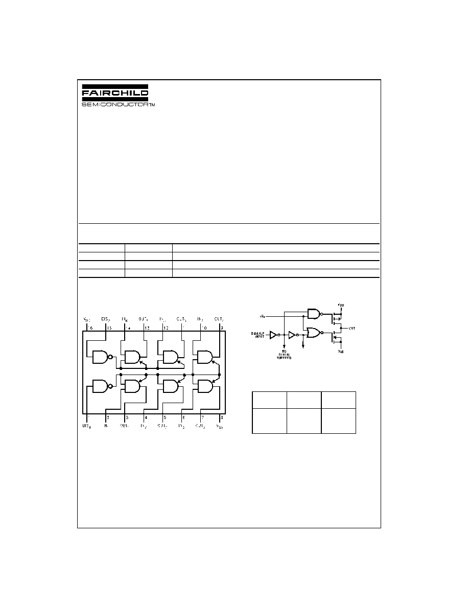
The CD4503BC is a hex non-inverting 3-STATE buffer with
high output current sink and source capability. 3-STATE
outputs make it useful in bus-oriented applications. Two
separate disable inputs are provided. Buffers 1 through 4
are controlled by the disable 4 input. Buffers 5 and 6 are
controlled by the disable 2 input. A high level on either dis-
able input will cause those gates on its control line to go
into a high impedance state.
Features
s
Wide supply voltage range:
3.0 V
DC
to 18 V
DC
s
3-STATE outputs
s
Symmetrical turn on/turn off delays
s
Symmetrical output rise and fall times
s
Pin-for-pin replacement for MM80C97 and MC14503
Ordering Code:
Devices also available in Tape and Reel. Specify by appending suffix letter "X" to the ordering code.
Connection Diagram
Pin Assignments for DIP, SOIC and SOP
Top View
Schematic Diagram
Truth Table
X
=
Don't Care
Order Number
Package Number
Package Description
CD4503BCM
M16A
16-Lead Small Outline Integrated Circuit (SOIC), JEDEC MS-012, 0.150" Narrow Body
CD4503BCSJ
M16D
16-Lead Small Outline Package (SOP), EIAJ TYPE II, 5.3mm Wide
CD4503BCN
N16E
16-Lead Plastic Dual-In-Line Package (PDIP), JEDEC MS-001, 0.300" Wide
In
Disable
Out
Input
0
0
0
1
0
1
X
1
3-STATE
www.fairchildsemi.com
2
C
D
45
03BC
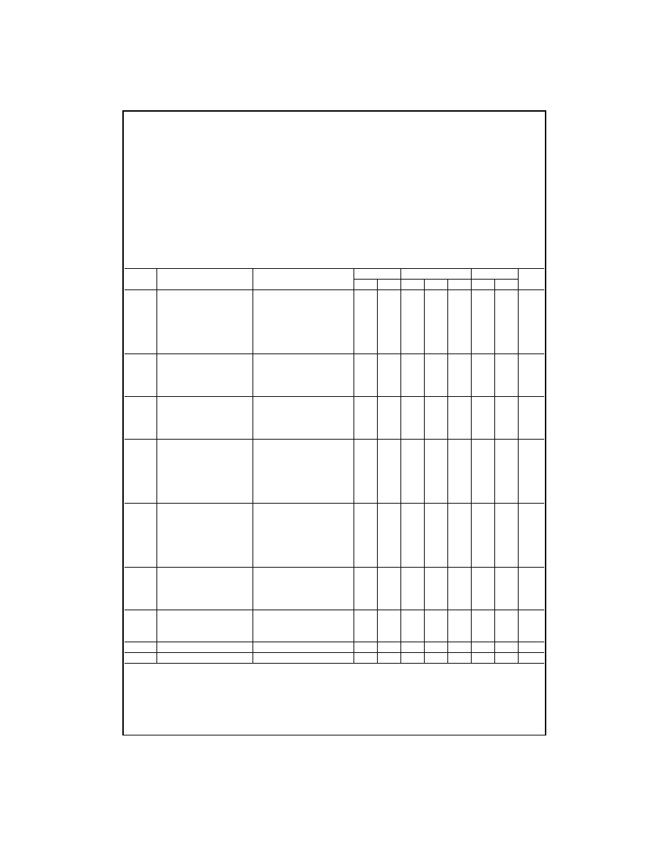
Absolute Maximum Ratings
(Note 1)
(Note 2)
Recommended Operating
Conditions
(Note 2)
Note 1: "Absolute Maximum Ratings" are those values beyond which the
safety of the device cannot be guaranteed. They are not meant to imply
that the devices should be operated at these limits. The tables of "Recom-
mended Operating Conditions" and "Electrical Characteristics" provide con-
ditions for actual device operation.
Note 2: V
SS
=
0V unless otherwise specified.
DC Electrical Characteristics
(Note 2)
Note 3: I
OH
and I
OL
are tested one output at a time.
Supply Voltage (V
DD
)
-
0.5V to
+
18V
Input Voltage (V
IN
)
-
0.5V to
+
0.5V
Storage Temperature Range (T
S
)
-
65
∞
C to
+
150
∞
C
Power Dissipation (P
D
)
Dual-In-Line
700 mW
Small Outline
500 mW
Lead Temperature (T
L
)
(Soldering, 10 seconds)
260
∞
C
Supply Voltage (V
DD
)
+
3V to
+
15V
Operating Temperature Range (T
A
)
-
40
∞
C to
+
85
∞
C
Symbol
Parameter
Conditions
-
40
∞
C
+
25
∞
C
+
85
∞
C
Units
Min
Max
Min
Typ
Max
Min
Max
I
DD
Quiescent Device
V
DD
=
5V,
4
4
30
µ
A
Current
V
IN
=
V
DD
or V
SS
V
DD
=
10V,
8
8
60
µ
A
V
IN
=
V
DD
or V
SS
V
DD
=
15V,
16
16
120
µ
A
V
IN
=
V
DD
or V
SS
V
OL
LOW Level
V
IN
=
V
DD
or 0
Output Voltage
V
DD
=
5V
0.05
0
0.05
0.05
V
V
DD
=
10V
0.05
0
0.05
0.05
V
V
DD
=
15V
0.05
0
0.05
0.05
V
V
OH
HIGH Level
V
IN
=
V
DD
or 0
Output Voltage
V
DD
=
5V
4.95
4.95
4.95
V
V
DD
=
10V
9.95
9.95
9.95
V
V
DD
=
15V
14.95
14.95
14.95
V
V
IL
LOW Level
V
DD
=
5V,
1.5
2.25
1.5
1.5
V
Input Voltage
V
O
=
4.5V or 0.5V
V
DD
=
10V,
3.0
4.50
3.0
3.0
V
V
O
=
9.0V or 1.0V
V
DD
=
15V,
4.0
6.75
4.0
4.0
V
V
O
=
13.5V or 1.5V
V
IH
HIGH Level
V
DD
=
5V,
3.5
3.5
2.75
3.5
V
Input Voltage
V
O
=
0.5V or 4.5V
V
DD
=
10V,
7.0
7.0
5.5
7.0
V
V
O
=
1.0V or 9.0V
V
DD
=
15V,
11.0
11.0
8.25
11.0
V
V
O
=
1.5V or 13.5V
I
OL
LOW Level Output
V
DD
=
4.5V, V
OL
=
0.4V
2.30
1.95
2.65
1.60
mA
Current V
DD
=
5.0V, V
OL
=
0.4V
2.5
2.10
2.75
1.75
mA
V
DD
=
10V, V
OL
=
0.5V
6.5
5.45
7.0
4.45
mA
V
DD
=
15V, V
OL
=
1.5V
16.50
13.80
25.00
11.30
mA
I
OH
HIGH Level Output
V
DD
=
5V, V
OH
=
4.6V
-
1.04
-
0.88
-
1.76
-
0.7
mA
Current V
DD
=
10V, V
OH
=
9.5V
-
2.60
-
2.2
-
4.50
-
1.8
mA
V
DD
=
15V, V
OH
=
13.5V
-
7.2
-
6.0
-
17.6
-
4.8
mA
I
TL
3-STATE Leakage Current
V
DD
=
15V
±
0.3
±
10
-
4
±
0.3
±
1.0
µ
A
I
IN
Input Current
V
DD
=
15V
±
0.3
±
10
-
5
±
0.3
±
1.0
µ
A
3
www.fairchildsemi.com
CD450
3BC
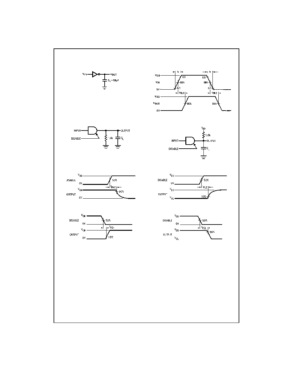
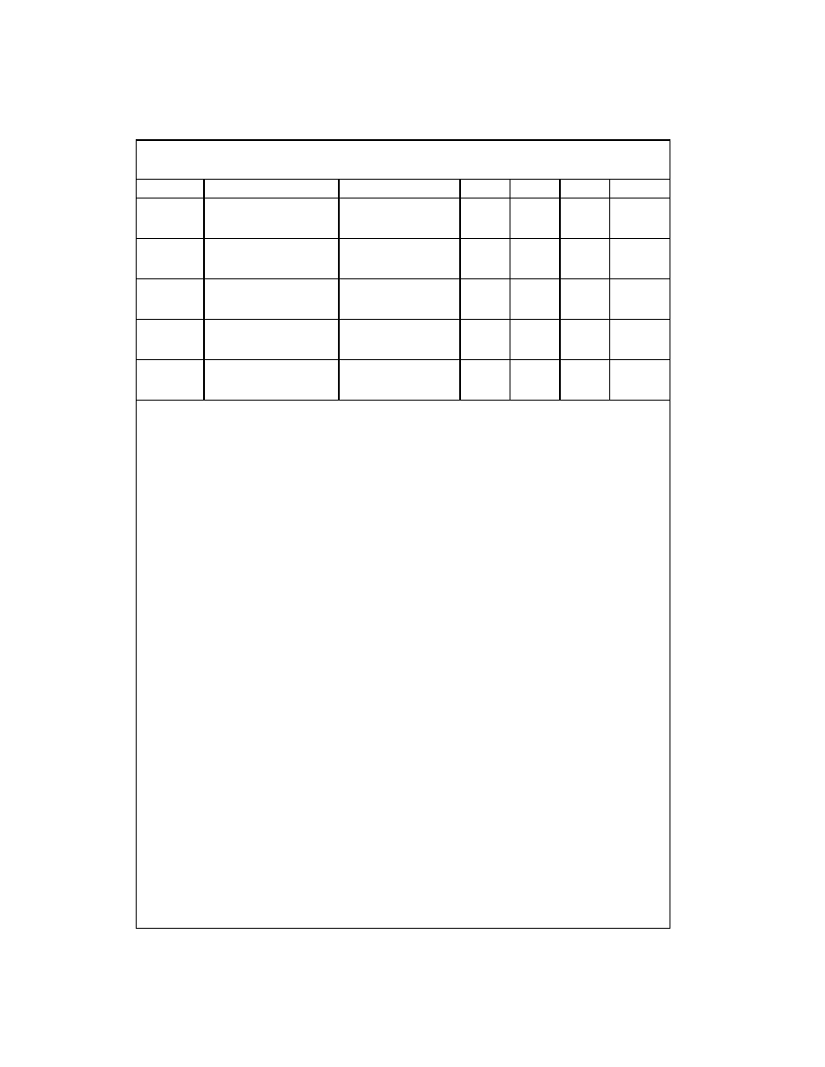
AC Electrical Characteristics
(Note 4)
T
A
=
25
∞
C, C
L
=
50 pF, R
L
=
200 k
, Input t
r
=
t
f
=
20 ns, unless otherwise specified
Note 4: AC Parameters are guaranteed by DC correlated testing.
Symbol
Parameter
Conditions
Min
Typ
Max
Units
t
PHL
, t
PLH
Propagation Delay Time
V
DD
=
5V
75
100
ns
V
DD
=
10V
35
40
ns
V
DD
=
15V
25
30
ns
t
PLZ
, t
PHZ
Propagation Delay Time,
V
DD
=
5V
80
125
ns
Logical Level to HIGH
V
DD
=
10V
40
90
ns
Impedance State
V
DD
=
15V
35
70
ns
t
PZL
, t
PZH
Propagation Delay Time,
V
DD
=
5V
95
175
ns
High Impedance State to
V
DD
=
10V
40
80
ns
Logical Level
V
DD
=
15V
35
70
ns
t
TLH
Output Rise Time
V
DD
=
5V
45
80
ns
V
DD
=
10V
23
40
ns
V
DD
=
15V
18
35
ns
t
THL
Output Fall Time
V
DD
=
5V
45
80
ns
V
DD
=
10V
23
40
ns
V
DD
=
15V
18
35
ns
5
www.fairchildsemi.com
CD450
3BC
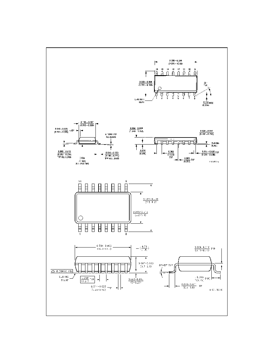
Physical Dimensions
inches (millimeters) unless otherwise noted
16-Lead Small Outline Integrated Circuit (SOIC), JEDEC MS-012, 0.150" Narrow
Package Number M16A
16-Lead Small Outline Package (SOP), EIAJ TYPE II, 5.3mm Wide
Package Number M16D