© 2002 Fairchild Semiconductor Corporation
DS005994
www.fairchildsemi.com
October 1987
Revised April 2002
CD451
4BC
·
CD4515BC
4
-
Bit
Latched/
4-
to-
16
L
i
ne Decoders
CD4514BC· CD4515BC
4-Bit Latched/4-to-16 Line Decoders
General Description
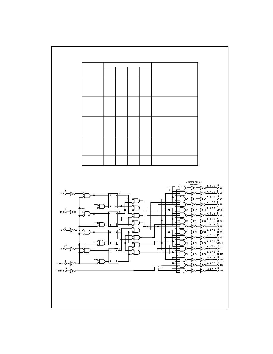
The CD4514BC and CD4515BC are 4-to-16 line decoders
with latched inputs implemented with complementary MOS
(CMOS) circuits constructed with N- and P-channel
enhancement mode transistors. These circuits are prima-
rily used in decoding applications where low power dissipa-
tion and/or high noise immunity is required.
The CD4514BC (output active high option) presents a logi-
cal "1" at the selected output, whereas the CD4515BC pre-
sents a logical "0" at the selected output. The input latches
are RS type flip-flops, which hold the last input data pre-
sented prior to the strobe transition from "1" to "0". This
input data is decoded and the corresponding output is acti-
vated. An output inhibit line is also available.
Features
s
Wide supply voltage range:
3.0V to 15V
s
High noise immunity:
0.45 V
DD
(typ.)
s
Low power TTL:
fan out of 2
compatibility:
driving 74L
s
Low quiescent power dissipation:
0.025
µ
W/package @ 5.0 V
DC
s
Single supply operation
s
Input impedance
=
10
12
typically
s
Plug-in replacement for MC14514, MC14515
Ordering Code:
Devices also available in Tape and Reel. Specify by appending suffix letter "X" to the ordering code.
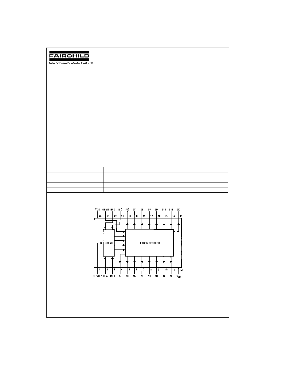
Connection Diagram
Top View
Order Number
Package Number
Package Diagram
CD4514BCWM
M24B
24-Lead Small Outline Integrated Circuit (SOIC), JEDEC MS-013, 0.300" Wide
CD4514BCN
N24A
24-Lead Plastic Dual-In-Line Package (PDIP), JEDEC MS-010, 0.600" Wide
CD4515BCWM
M24B
24-Lead Small Outline Integrated Circuit (SOIC), JEDEC MS-013, 0.300" Wide
CD4515BCN
N24A
24-Lead Plastic Dual-In-Line Package (PDIP), JEDEC MS-010, 0.600" Wide
3
www.fairchildsemi.com
CD451
4BC
·
CD4515BC
Absolute Maximum Ratings
(Note 1)
(Note 2)
Recommended Operating
Conditions
(Note 2)
Note 1: "Absolute Maximum Ratings" are those values beyond which the
safety of the device cannot be guaranteed. Except for "Operating Tempera-
ture Range" they are not meant to imply that the devices should be oper-
ated at these limits. The tables of "Recommended Operating Conditions"
and "Electrical Characteristics" provide conditions for actual device opera-
tion.
Note 2: V
SS
=
0V unless otherwise specified.
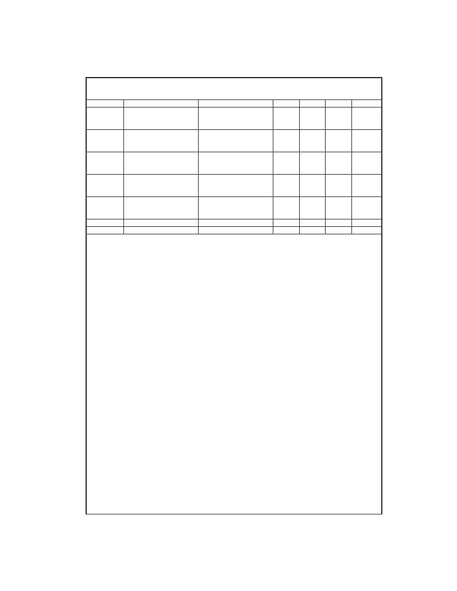
DC Electrical Characteristics
(Note 2)
CD4514BC, CD4515BC
Note 3: I
OH
and I
OL
are tested one output at a time.
DC Supply Voltage (V
DD
)
-
0.5V to
+
18V
Input Voltage (V
IN
)
-
0.5V to V
DD
+
0.5V
Storage Temperature Range (T
S
)
-
65
°
C to
+
150
°
C
Power Dissipation (P
D
)
Dual-In-Line
700 mW
Small Outline
500 mW
Lead Temperature (T
L
)
(Soldering, 10 seconds)
260
°
C
DC Supply Voltage (V
DD
)
3V to 15V
Input Voltage (V
IN
)
0V to V
DD
Operating Temperature Range (T
A
)
CD4514BC,
CD4515BC
-
55
°
C to
+
125
°
C
Symbol
Parameter
Conditions
-
55
°
C
+
25
°
C
+
125
°
C
Units
Min
Max
Min
Typ
Max
Min
Max
I
DD
Quiescent Device
V
DD
=
5V, V
IN
=
V
DD
or V
SS
5
0.005
5
150
µ
A
Current
V
DD
=
10V, V
IN
=
V
DD
or V
SS
10
0.010
10
300
V
DD
=
15V, V
IN
=
V
DD
or V
SS
20
0.015
20
600
V
OL
LOW Level
V
IL
=
0V, V
IH
=
V
DD
,
Output Voltage
|I
O
|
<
1
µ
A
V
DD
=
5V
0.05
0
0.05
0.05
V
V
DD
=
10V
0.05
0
0.05
0.05
V
DD
=
15V
0.05
0
0.05
0.05
V
OH
HIGH Level
V
IL
=
0V, V
IH
=
V
DD
,
Output Voltage
|I
O
|
<
1
µ
A
V
DD
=
5V
4.95
4.95
5.0
4.95
V
V
DD
=
10V
9.95
9.95
10.0
9.95
V
DD
=
15V
14.95
14.95
15.0
14.95
V
IL
LOW Level
|I
O
|
<
1
µ
A
Input Voltage
V
DD
=
5V, V
O
=
0.5V or 4.5V
1.5
2.25
1.5
1.5
V
V
DD
=
10V, V
O
=
1.0V or 9.0V
3.0
4.50
3.0
3.0
V
DD
=
15V, V
O
=
1.5V or 13.5V
4.0
6.75
4.0
4.0
V
IH
HIGH Level
|I
O
|
<
1
µ
A
Input Voltage
V
DD
=
5V, V
O
=
0.5V or 4.5V
3.5
3.5
2.75
3.5
V
V
DD
=
10V, V
O
=
1.0V or 9.0V
7.0
7.0
5.50
7.0
V
DD
=
15V, V
O
=
1.5V or 13.5V
11.0
11.0
8.25
11.0
I
OL
LOW Level Output
V
DD
=
5V, V
O
=
0.4V
0.64
0.51
0.88
0.36
mA
Current (Note 3)
V
DD
=
10V, V
O
=
0.5V
1.6
1.3
2.25
0.90
V
DD
=
15V, V
O
=
1.5V
4.2
3.4
8.8
2.4
I
OH
HIGH Level Output
V
DD
=
5V, V
O
=
4.6V
-
0.64
-
0.51
-
0.88
-
0.36
mA
Current (Note 3)
V
DD
=
10V, V
O
=
9.5V
-
1.6
-
1.3
-
2.25
-
0.90
V
DD
=
15V, V
O
=
13.5V
-
4.2
-
3.4
-
8.8
-
2.4
I
IN
Input Current
V
DD
=
15V, V
IN
=
0V
-
0.1
-
10
-
5
-
0.1
-
1.0
µ
A
V
DD
=
15V, V
IN
=
15V
0.1
10
-
5
0.1
1.0
www.fairchildsemi.com
4
CD4514BC
·
C
D
45
15BC
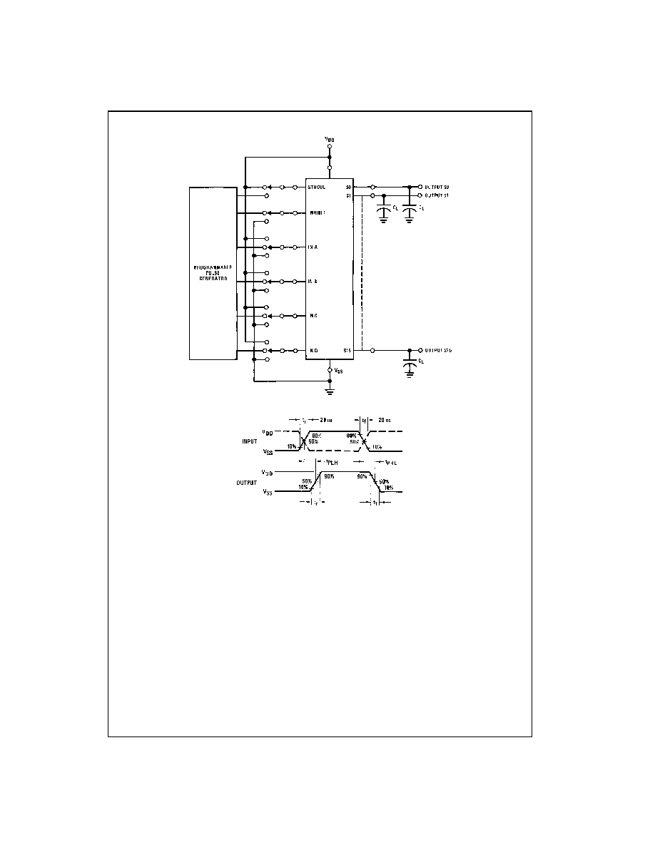
AC Electrical Characteristics
(Note 4)
All types C
L
=
50 pF, T
A
=
25
°
C, t
r
=
t
f
=
20 ns unless otherwise specified
Note 4: AC Parameters are guaranteed by DC correlated testing.
Note 5: C
PD
determines the no load AC power consumption of any CMOS device. For complete explanation, see Family Characteristics application note,
AN-90.
Note 6: Capacitance is guaranteed by periodic testing.
Symbol
Parameter
Conditions
Min
Typ
Max
Units
t
THL
, t
TLH
Transition Times
V
DD
=
5V
100
200
ns
V
DD
=
10V
50
100
V
DD
=
15V
40
80
t
PLH
, t
PHL
Propagation Delay Times
V
DD
=
5V
550
1100
ns
V
DD
=
10V
225
450
V
DD
=
15V
150
300
t
PLH
, t
PHL
Inhibit Propagation
V
DD
=
5V
400
800
ns
Delay Times
V
DD
=
10V
150
300
V
DD
=
15V
100
200
t
SU
Setup Time
V
DD
=
5V
125
250
ns
V
DD
=
10V
50
100
V
DD
=
15V
38
75
t
WH
Strobe Pulse Width
V
DD
=
5V
175
350
ns
V
DD
=
10V
50
100
V
DD
=
15V
38
75
C
PD
Power Dissipation Capacitance
Per Package (Note 5)
150
pF
C
IN
Input Capacitance
Any Input (Note 6)
5
7.5
pF