October 1987
Revised January 1999
CD472
4BC
8-
B
i
t
Ad
dres
sab
le Lat
c
h
© 1999 Fairchild Semiconductor Corporation
DS006003.prf
www.fairchildsemi.com
CD4724BC
8-Bit Addressable Latch
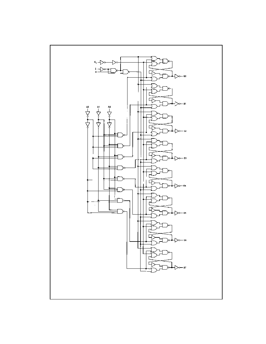
General Description
The CD4724BC is an 8-bit addressable latch with three
address inputs (A0≠A2), an active low enable input (E),
active high clear input (CL), a data input (D) and eight out-
puts (Q0≠Q7).
Data is entered into a particular bit in the latch when that is
addressed by the address inputs and the enable (E) is
LOW. Data entry is inhibited when enable (E) is HIGH.
When clear (CL) and enable (E) are HIGH, all outputs are
LOW. When clear (CL) is HIGH and enable (E) is LOW, the
channel demultiplexing occurs. The bit that is addressed
has an active output which follows the data input while all
unaddressed bits are held LOW. When operating in the
addressable latch mode (E
=
CL
=
LOW), changing more
than one bit of the address could impose a transient wrong
address. Therefore, this should only be done while in the
memory mode (E
=
HIGH, CL
=
LOW).
Features
s
Wide supply voltage range:
3.0V to 15V
s
High noise immunity:
0.45 V
DD
(typ.)
s
Low power TTL compatibility:
fan out of 2 driving 74L or 1 driving 74LS
s
Serial to parallel capability
s
Storage register capability
s
Random (addressable) data entry
s
Active high demultiplexing capability
s
Common active high clear
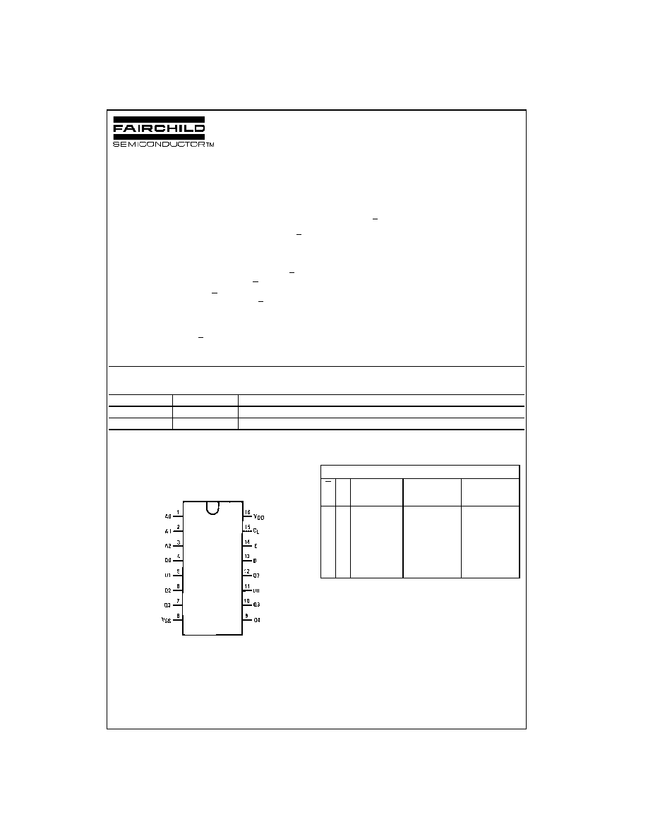
Ordering Code:
Devices also available in Tape and Reel. Specify by appending the suffix letter "X" to the ordering code.
Connection Diagram
Pin Assignments for DIP and SOIC
Top View
Truth Table
Order Number
Package Number
Package Description
CD4724BCM
M16A
16-Lead Small Outline Integrated Circuit (SOIC), JEDEC MS-012, 0.150" Narrow Body
CD4724BCN
N16E
16-Lead Plastic Dual-In-Line Package (PDIP), JEDEC MS-001, 0.300" Wide
Mode Selection
E
CL
Addressed
Unaddressed
Mode
Latch
Latch
L
L
Follows Data
Holds Previous
Data
Addressable
Latch
H
L
Hold Previous
Data
Holds Previous
Data
Memory
L
H
Follows Data
Reset to "0"
Demultiplexer
H
H
Reset to "0"
Reset to "0"
Clear
3
www.fairchildsemi.com
CD472
4BC
Absolute Maximum Ratings
(Note 1)
(Note 2)
Recommended Operating
Conditions
(Note 2)
Note 1: "Absolute Maximum Ratings" are those values beyond which the
safety of the device cannot be guaranteed; they are not meant to imply that
the devices should be operated at these limits. The tables of "Recom-
mended Operating Conditions" and Electrical Characteristics" provide con-
ditions for actual device operation.
Note 2: V
SS
=
0V unless otherwise specified.
DC Electrical Characteristics
(Note 2)
Note 3: I
OL
and I
OH
are tested one output at a time.
DC Supply Voltage (V
DD
)
-
0.5V to
+
18 V
DC
Input Voltage (V
IN
)
-
0.5V to V
DD
+
0.5 V
DC
Storage Temperature (T
S
)
-
65
∞
C to
+
150
∞
C
Power Dissipation (P
D
)
Dual-In-Line
700 mW
Small Outline
500 mW
Lead Temperature (T
L
)
(Soldering, 10 seconds)
260
∞
C
DC Supply Voltage (V
DD
)
3.0V to 15 V
DC
Input Voltage (V
IN
)
0V to V
DD
V
DC
Operating Temperature Range (T
A
)
-
40
∞
C to
+
85
∞
C
Symbol
Parameter
Conditions
-
40
∞
C
+
25
∞
C
+
85
∞
C
Units
Min
Max
Min
Typ
Max
Min
Max
I
DD
Quiescent Device
V
DD
=
5V
20
0.02
20
150
µ
A
Current
V
DD
=
10V
40
0.02
40
300
µ
A
V
DD
=
15V
80
0.02
80
600
µ
A
V
OL
LOW Level
|I
O
|
1
µ
A
Output Voltage
V
DD
=
5V
0.05
0
0.05
0.05
V
V
DD
=
10V
0.05
0
0.05
0.05
V
V
DD
=
15V
0.05
0
0.05
0.05
V
V
OH
HIGH Level
|I
O
|
1
µ
A
Output Voltage
V
DD
=
5V
4.95
4.95
5.0
4.95
V
V
DD
=
10V
9.95
9.95
10
9.95
V
V
DD
=
15V
14.95
14.95
15
14.95
V
V
IL
LOW Level
V
DD
=
5V, V
O
=
0.5V or 4.5V
1.5
2.25
1.5
1.5
V
Input Voltage
V
DD
=
10V, V
O
=
1V or 9V
3.0
4.5
3.0
3.0
V
V
DD
=
15V, V
O
=
1.5V or 13.5V
4.0
6.75
4.0
4.0
V
V
IH
HIGH Level
V
DD
=
5V, V
O
=
0.5V or 4.5V
3.5
3.5
2.75
3.5
V
Input Voltage
V
DD
=
10V, V
O
=
1V or 9V
7.0
7.0
5.5
7.0
V
V
DD
=
15V, V
O
=
1.5V or 13.5V
11.0
11.0
8.25
11.0
V
I
OL
LOW Level Output
V
DD
=
5V, V
O
=
0.4V
0.52
0.44
0.88
0.36
mA
Current
V
DD
=
10V, V
O
=
0.5V
1.3
1.1
2.25
0.9
mA
(Note 3)
V
DD
=
15V, V
O
=
1.5V
3.6
3.0
8.8
2.4
mA
I
OH
HIGH Level Output
V
DD
=
5V, V
O
=
4.6V
-
0.52
-
0.44
-
0.88
-
0.36
mA
Current
V
DD
=
10V, V
O
=
9.5V
-
1.3
-
1.1
-
2.25
-
0.9
mA
(Note 3)
V
DD
=
15V, V
O
=
13.5V
-
3.6
-
3.0
-
8.8
-
2.4
mA
I
IN
Input Current
V
DD
=
15V, V
IN
=
0V
-
0.30
-
10
-
5
-
0.30
-
1.0
µ
A
V
DD
=
15V, V
IN
=
15V
0.30
10
-
5
0.30
1.0
µ
A
www.fairchildsemi.com
4
C
D
47
24BC
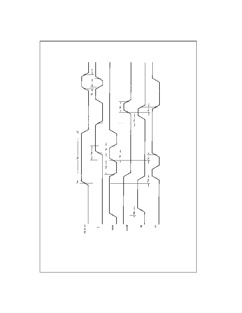
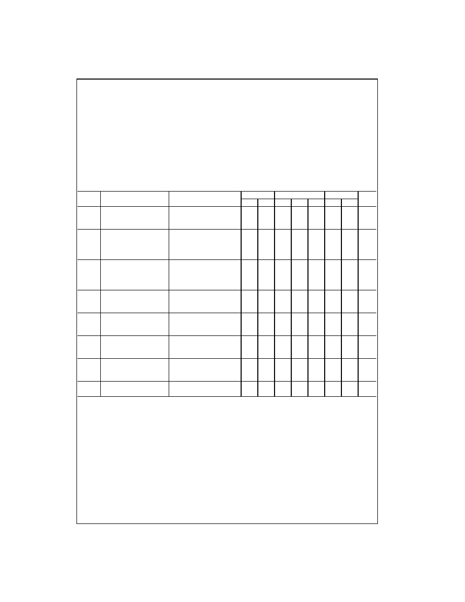
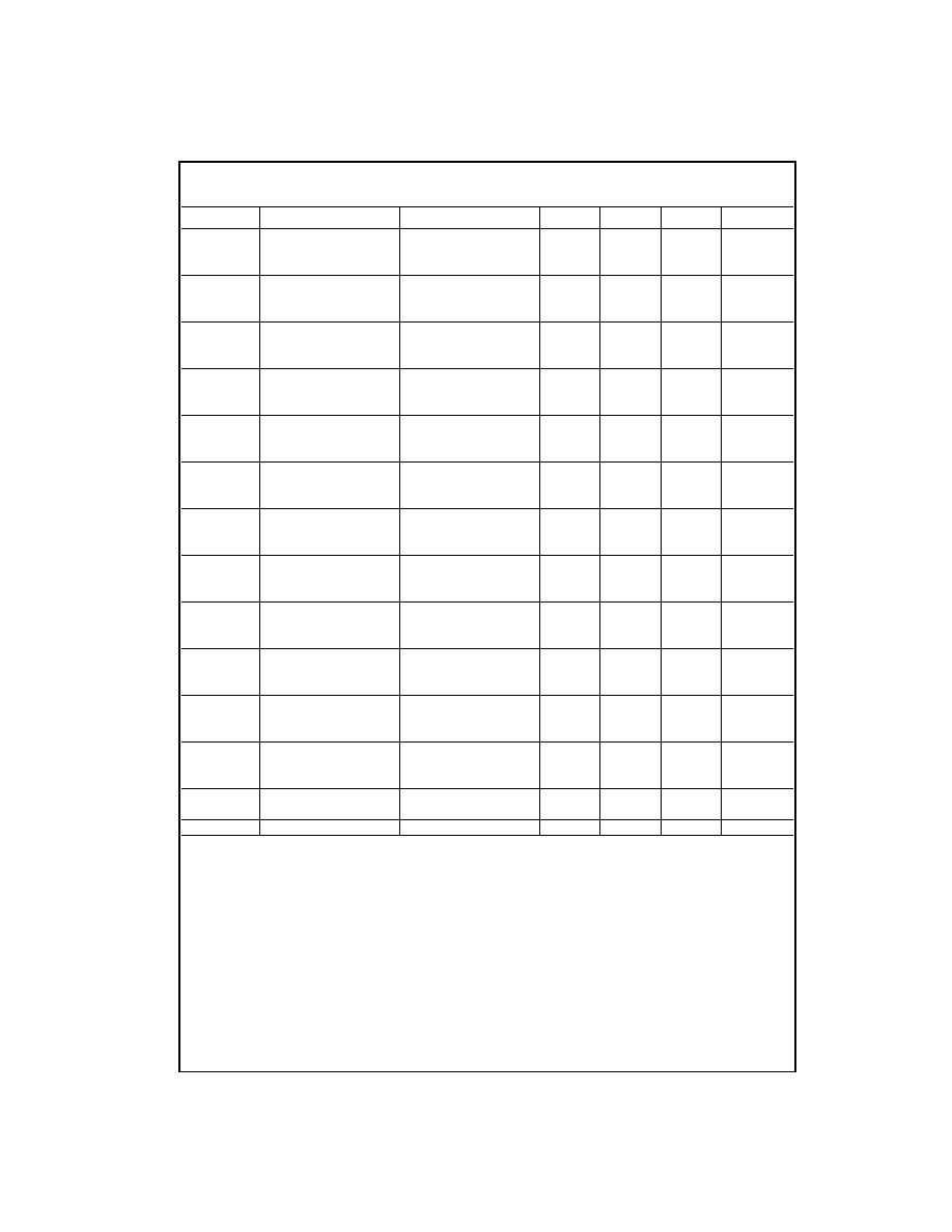
AC Electrical Characteristics
(Note 4)
T
A
=
25
∞
C, C
L
=
50 pF, R
L
=
200k, Input t
r
=
t
f
=
20 ns, unless otherwise noted
Note 4: AC Parameters are guaranteed by DC correlated testing.
Note 5: Dynamic power dissipation (P
D
) is given by: P
D
=
(C
PD
+
C
L
) V
CC
2
f
+
P
Q
; where C
L
=
load capacitance; f
=
frequency of operation; for further details,
see Application Note AN-90, "Family Characteristics".
Symbol
Parameter
Conditions
Min
Typ
Max
Units
t
PHL, tPLH
Propagation Delay
V
DD
=
5V
200
400
ns
Data to Output
V
DD
=
10V
75
150
ns
V
DD
=
15V
50
100
ns
t
PLH
, t
PHL
Propagation Delay
V
DD
=
5V
200
400
ns
Enable to Output
V
DD
=
10V
80
160
ns
V
DD
=
15V
60
120
ns
t
PHL
Propagation Delay
V
DD
=
5V
175
350
ns
Clear to Output
V
DD
=
10V
80
160
ns
V
DD
=
15V
65
130
ns
t
PLH
, t
PHL
Propagation Delay
V
DD
=
5V
225
450
ns
Address to Output
V
DD
=
10V
100
200
ns
V
DD
=
15V
75
150
ns
t
THL
, t
TLH
Transition Time
V
DD
=
5V
100
200
ns
(Any Output)
V
DD
=
10V
50
100
ns
V
DD
=
15V
40
80
ns
T
WH
, T
WL
Minimum Data
V
DD
=
5V
100
200
ns
Pulse Width
V
DD
=
10V
50
100
ns
V
DD
=
15V
40
80
ns
t
WH
, t
WL
Minimum Address
V
DD
=
5V
200
400
ns
Pulse Width
V
DD
=
10V
100
200
ns
V
DD
=
15V
65
125
ns
t
WH
Minimum Clear
V
DD
=
5V
75
150
ns
Pulse Width
V
DD
=
10V
40
75
ns
V
DD
=
15V
25
50
ns
t
SU
Minimum Setup Time
V
DD
=
5V
40
80
ns
Data to E
V
DD
=
10V
20
40
ns
V
DD
=
15V
15
30
ns
t
H
Minimum Hold Time
V
DD
=
5V
60
120
ns
Data to E
V
DD
=
10V
30
60
ns
V
DD
=
15V
25
50
ns
t
SU
Minimum Setup Time
V
DD
=
5V
-
15
50
ns
Address to E
V
DD
=
10V
0
30
ns
V
DD
=
15V
0
20
ns
t
H
Minimum Hold Time
V
DD
=
5V
-
50
15
ns
Address to E
V
DD
=
10V
-
20
10
ns
V
DD
=
15V
-
15
5
ns
C
PD
Power Dissipation
Per Package
100
pF
Capacitance
(Note 5)
C
IN
Input Capacitance
Any Input
5.0
7.5
pF