 | ÐлекÑÑоннÑй компоненÑ: CGS3321CW | СкаÑаÑÑ:  PDF PDF  ZIP ZIP |
CGS3321 * CGS3322 CMOS Crystal Clock Generators
© 2001 Fairchild Semiconductor Corporation
DS011503
www.fairchildsemi.com
September 1195
Revised January 2001
CGS3321 ·
CGS3322 CMO
S
Cryst
al Clo
ck
Gener
a
tor
s
CGS3321 · CGS3322
CMOS Crystal Clock Generators
General Description
The CGS3321 and CGS3322 devices are designed for
Clock Generation and Support (CGS) applications up to
110 MHz. The CGS332x series of devices are crystal con-
trolled CMOS oscillators requiring a minimum of external
components. The 332x devices provide selectable output
divide ratio. The circuit is designed to operate over a wide
frequency range using fundamental mode or overtone crys-
tals.
Features
s
Fairchild's CGS family of devices for high frequency
clock source applications
s
Crystal frequency operation range:
fundamental: 10 MHz to 100 MHz typical
3rd or 5th overtone: 10 MHz to 95 MHz
s
1000V ESD protection on OCS_IN and OSC_OUT pins.
2000V ESD protection on all other pins
s
Output current drive of 48 mA for I
OL
/I
OH
s
FACT
CMOS output levels
s
Output has high speed short circuit protection
s
Intended for Pierce oscillator applications
s
Hysteresis inputs to improve noise margin
s
CGS3321 has duty cycle adjust
s
CGS3322 has 1, 2, 4 divide ratio
Ordering Code:
Devices also available in Tape and Reel. Specify by appending the suffix letter "X" to the ordering code.
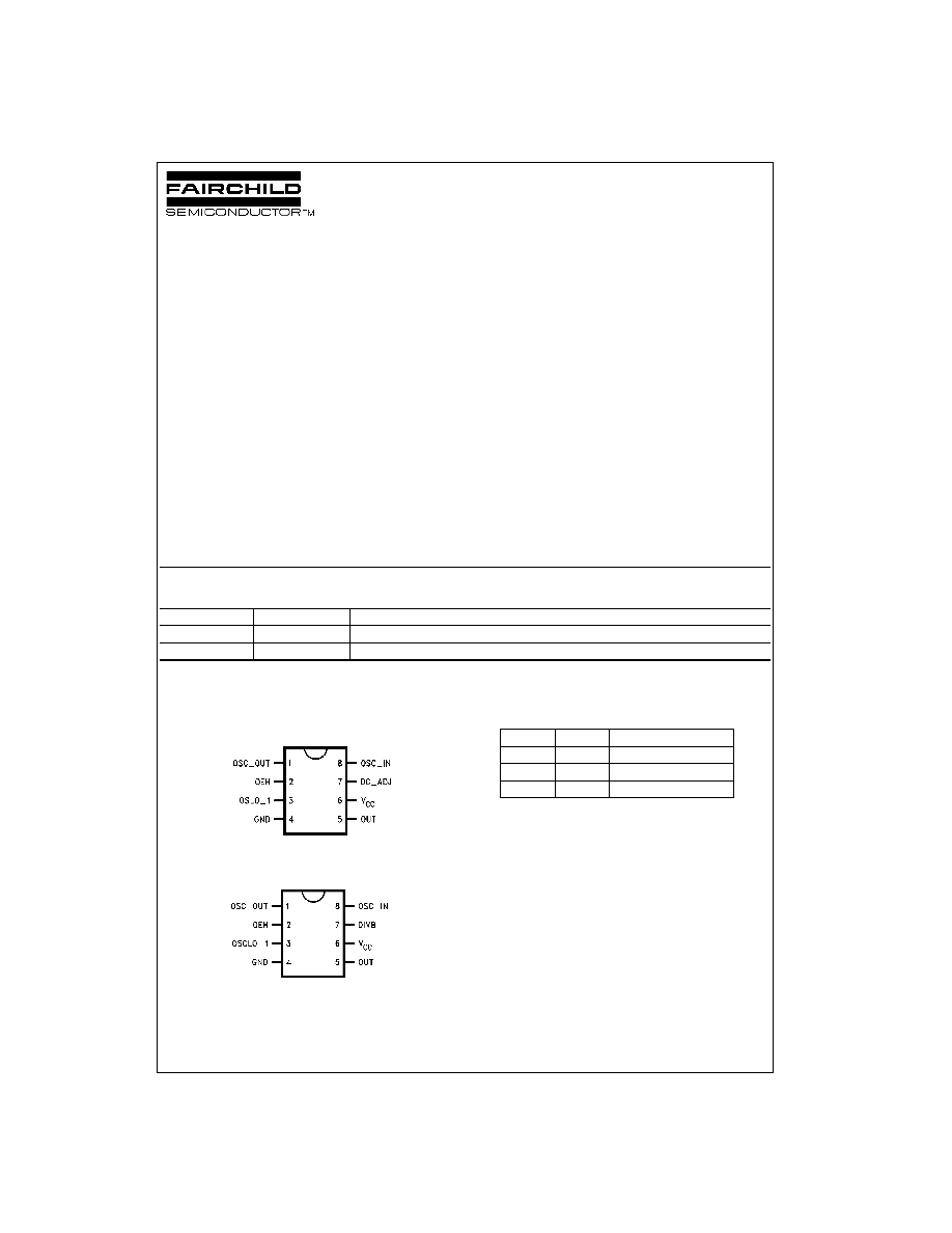
Connection Diagrams
CGS3321
CGS3322
Truth Table
Division Selection
Note: Actual value of the floating DIVB input is V
CC/2
FACT
is a trademark of Fairchild Semiconductor Corporation.
Order Number
Package Number
Package Description
CGS3321M
M08A
8-Lead Small Outline Integrated Circuit (SOIC), JEDEC MS-012, 0.150" Narrow
CGS3322M
M08A
8-Lead Small Outline Integrated Circuit (SOIC), JEDEC MS-012, 0.150" Narrow
DIVB
OEH
Divider Output
F
X
Divide-by 1
1
1
Divide-by 2
0
1
Divide-by 4

www.fairchildsemi.com
2
C
G
S3321
·
C
G
S3322
Pin Descriptions
Note: Pin out varies for each device.
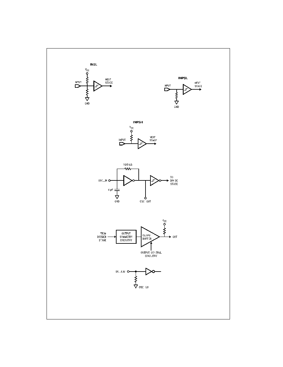
Block Diagrams
Note: Pin numbers vary for each device
Note: Pin out varies for each device.
OSC_IN
Input to Oscillator Inverter. The output of the
crystal would be connected here.
OEH
Active HIGH 3-STATE enable pin. This pin pulls
to a HIGH value when left floating and 3-
STATEs the output when forced LOW. This pin
has TTL compatible input levels.
OSC_OUT Resistive Buffered Output of the Oscillator
Inverter
OUT
This pin is the main clock output on the device.
DIVB
(CGS3322 only)
3-Level input used to select Binary Divide-by
value of output frequency.
OSCLO_1
The Oscillator LOW pin is the ground for the
Oscillator.
DC_ADJ
(CGS3321 only)
Active high input that controls output duty
cycle. Logic high level will delay the HL transi-
tion edge approximately 0.3 ns.
V
CC
The power pin for the chip.
GND
The ground pin for all sections of the circuitry
except the oscillator and oscillator related
circuitry.
3
www.fairchildsemi.com
CGS3321
·
CGS3322
Block Diagrams
(Continued)
Oscillator Stage
Output Stage
www.fairchildsemi.com
4
C
G
S3321
·
C
G
S3322
Absolute Maximum Ratings
(Note 1)
Recommended Operating
Conditions
Note 1: The Absolute Maximum Ratings are those values beyond which
the safety of the device cannot be guaranteed. The device should not be
operated at these limits. The parametric values defined in the DC and AC
Electrical Characteristics tables are not guaranteed at the absolute maxi-
mum ratings. The Recommended Operating Conditions will define the con-
ditions for actual device operation.
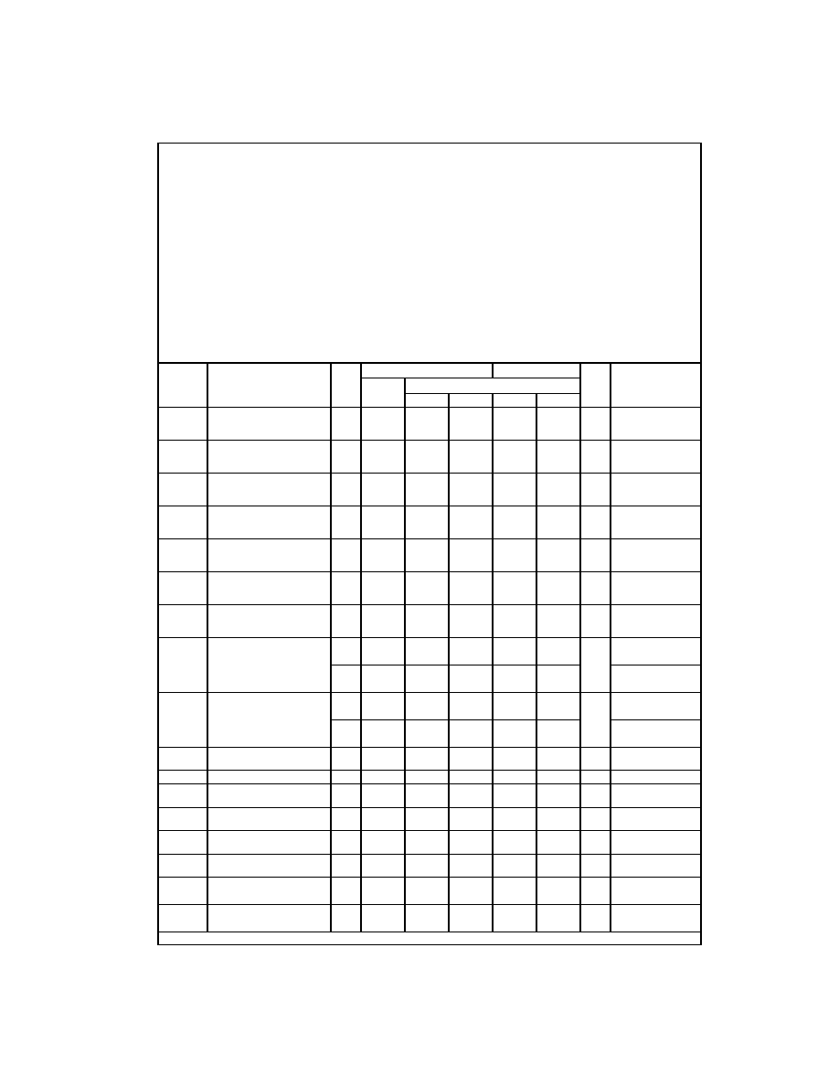
DC Electrical Characteristics
Supply Voltage (V
CC
)
-
0.5V to 7.0V
DC Input Voltage Diode Current (I
IK
)
±
9 mA
DC Input Voltage (V
I
)
-
0.5V to 7.0V
DC Output Diode Current (I
OK
)
±
20 mA
DC Output Voltage (V
O
)
-0.5V to V
CC
+
0.5V
DC Output Source
or Sink Current (I
O
)
±
70 mA
Storage Temperature (T
STG
)
-
55
°
C to 150
°
C
Junction Temperature (T
J
)
SOIC
140
°
C/W
Supply Voltage (V
CC
)
4.5V to 5.5V
Input Voltage (V
I
)
0V to 5.5V
Output Voltage (V
O
)
0V to V
CC
V
Operating Temperature (T
A
)
-
40
°
to
+
85
°
C
Symbol
Parameter
T
A
=
+
25
°
C
T
A
=
-
40
°
C to
+
85
°
C
Units
Conditions
V
CC
Typ
Guaranteed Limits
(V)
Min
Max
Min
Max
V
IHTTL
Minimum HIGH Level
Input Voltage,
TTL Level Inputs (OEH, OEL)
4.5
2.0
2.0
V
5.5
2.0
2.0
V
ILTTL
Maximum LOW Level
Input Voltage, TTL Level
Inputs (OEH, OEL)
4.5
0.8
0.8
V
5.5
0.8
0.8
V
IHCMOS
Minimum HIGH Level
Input Voltage. CMOS
Level Inputs (DC_ADJ)
4.5
3.15
3.15
V
5.5
3.85
3.85
V
ILCMOS
Maximum LOW Level
Input voltage. CMOS
Level Inputs (DC_ADJ)
4.5
1.35
1.35
V
5.5
1.65
1.65
V
IN3L_H
Minimum Logic 1 Input
for Three Level Input
(DIVB)
4.5
4.05
4.05
V
5.5
4.95
4.95
V
IN3L_1/2
Minimum Logic 1/2 Input
for Three Level Input
(DIVB)
4.5
1.8
2.7
1.8
2.7
V
5.5
2.2
3.3
2.2
3.3
V
IN3L_L
Maximum Logic 0 Input
Level Three Level Input
(DIVB)
4.5
0.45
0.45
V
5.5
0.45
0.45
V
OH
Minimum HIGH Level
Output Voltage
4.5
4.49
4.40
4.40
V
I
OUT
=
-
50
µ
A
5.5
5.49
5.40
5.40
4.5
3.86
3.76
I
OH
=
-
48 mA
5.5
4.86
4.76
V
IN
=
V
IH
or V
IH
V
OL
Minimum LOW Level
Output Voltage
4.5
0.001
0.1
0.1
V
I
OUT
=
50
µ
A
5.5
0.001
0.1
0.1
4.5
0.44
0.44
I
OL
=
+
48mA
5.5
0.44
0.44
V
IN
=
V
IL
or V
IH
I
IHRES
Input Current for Pins DIVB
5.5
220
360
200
380
µ
A
V
IN
=
5.5V
I
ILRES
Input Current for Pins DIVB
5.5
-
220
-
360
-
200
-
380
µ
A
VIN
=
0.0V
I
IHENAB
Input Current for
Enable Pin OEL
5.5
90
160
85
175
µ
A
V
IN
=
5.5V
I
ILENAB
Input Current for
Enable Pin OEH
5.5
-
90
-
160
-
85
-
175
µ
A
V
IN
=
0.0V
I
IHOSC
Input Current for OSC_IN Pin
(Indicates Bias Resistance)
5.5
20
100
20
125
µ
A
V
IN
=
5.5V
I
ILOSC
Input Current for OSC_IN Pin
(Indicates Bias Resistance)
5.5
-
20
-
100
-
20
-
125
µ
A
V
IN
=
0.0V
I
OZH
Output Disabled Current
4.5
3.0
5.0
µ
A
V
OUT
=
V
CC
(Output HIGH)
5.5
3.0
5.0
I
OZL
Output Disabled Current
4.5
-
140
-
150
µ
A
V
OUT
=
0.0V
(Output LOW)
5.5
-
170
-
180

5
www.fairchildsemi.com
CGS3321
·
CGS3322
DC Electrical Characteristics
(Continued)
AC Electrical Characteristics
Over recommended operating free air temperature range. All typical values are measured at V
CC
=
5V, T
A
=
25
°
C.
Note 2: Voltage Range 5.0 is 5.0V
±
0.5V
Symbol
Parameter
T
A
=
+
25
°
C
T
A
=
-
40
°
C to
+
85
°
C
Units
Conditions
V
CC
Typ
Guaranteed Limits
(V)
Min
Max
Min
Max
I
OLD
Minimum Dynamic
Output Current
5.5
75
75
mA
V
OLD
=
1.65V
I
OHD
Minimum Dynamic
Output Current
5.5
-
75
-
75
mA
V
OHD
=
3.85V
I
CCT
Additional Maximum I
CC
per Input
(OEH, OEL Pins)
5.5
1.5
1.5
mA
V
IN
=
V
CC
-
2.1V
I
CC3L
Additional Maximum I
CC
per Input
(DIVB)
5.5
1.5
1.5
mA
DIVB, OSC_DR
Inputs Equal to V
CC/2
Symbol
Parameter
V
CC
T
A
=
-
40
°
C to
+
85
°
C
Units
(V)
C
L
=
50 pF
(Note 2)
Min
Type
Max
f
MAX
Frequency Maximum
5.0
95
110
MHz
t
PZH
Output HIGH Enable Time
5.0
1.0
31.5
ns
t
PZL
Output LOW Enable Time
5.0
1.0
28.0
ns
t
PHZ
Output HIGH Disable Time
5.0
1.0
21.5
ns
t
PLZ
Output LOW Disable Time
5.0
1.0
16.0
ns
t
RISE
Rise/Fall Time
5.0
1.0
ns
t
FALL
30 pF (20% to 80%)