 | –≠–ª–µ–∫—Ç—Ä–æ–Ω–Ω—ã–π –∫–æ–º–ø–æ–Ω–µ–Ω—Ç: D45H8 | –°–∫–∞—á–∞—Ç—å:  PDF PDF  ZIP ZIP |
D45H8 / NZT45H8
D45H8
PNP Power Amplifier
This device is designed for power amplifier, regulator and switching
circuits where speed is important. Sourced from Process 5Q.
Absolute Maximum Ratings*
TA = 25∞C unless otherwise noted
Symbol
Parameter
Value
Units
V
CEO
Collector-Emitter Voltage
60
V
I
C
Collector Current - Continuous
8.0
A
T
J
, T
stg
Operating and Storage Junction Temperature Range
-55 to +150
∞
C
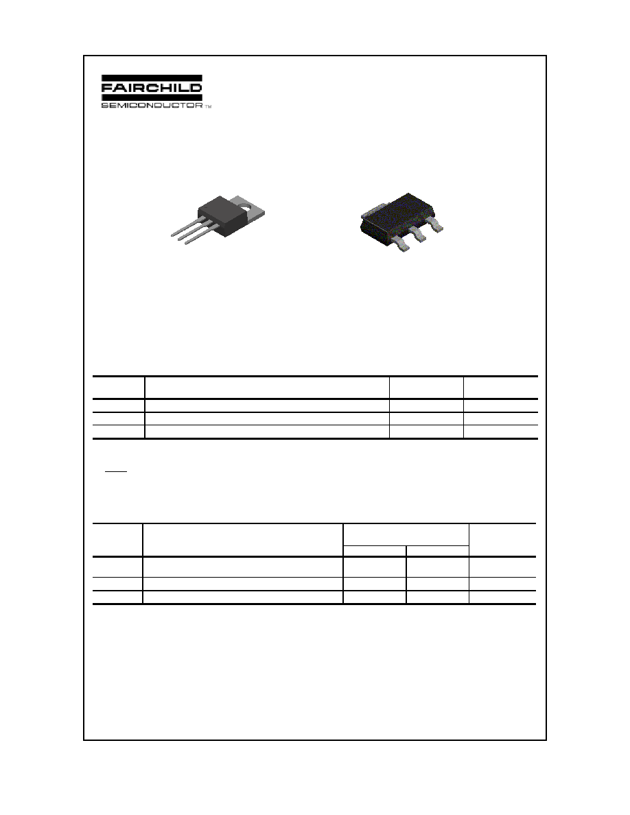
TO-220
B
C
E
B
C
C
SOT-223
E
NZT45H8
NOTES:
1) These ratings are based on a maximum junction temperature of 150 degrees C.
2) These are steady state limits. The factory should be consulted on applications involving pulsed or low duty cycle operations.
*
These ratings are limiting values above which the serviceability of any semiconductor device may be impaired.
Thermal Characteristics
TA = 25∞C unless otherwise noted
Symbol
Characteristic
Max
Units
D45H8
*NZT45H8
P
D
Total Device Dissipation
Derate above 25
∞
C
60
480
1.5
12
W
mW/
∞
C
R
JC
Thermal Resistance, Junction to Case
2.1
∞
C/W
R
JA
Thermal Resistance, Junction to Ambient
62.5
83.3
∞
C/W
*
Device mounted on FR-4 PCB 36 mm X 18 mm X 1.5 mm; mounting pad for the collector lead min. 6 cm
2
.
Discrete POWER & Signal
Technologies
©
1997 Fairchild Semiconductor Corporation
D45H8 / NZT45H8
Electrical Characteristics
TA = 25∞C unless otherwise noted
OFF CHARACTERISTICS
Symbol
Parameter
Test Conditions
Min
Max
Units
V
(BR)CEO
Collector-Emitter Breakdown Voltage
I
C
= 100 mA, I
B
= 0
60
V
I
CBO
Collector-Cutoff Current
V
CB
= 60 V, I
E
= 0
10
µ
A
I
EBO
Emitter-Cutoff Current
V
EB
= 5.0 V, I
C
= 0
100
µ
A
ON CHARACTERISTICS
SMALL SIGNAL CHARACTERISTICS
h
FE
DC Current Gain
I
C
= 2.0 A, V
CE
= 1.0 V
I
C
= 4.0 A, V
CE
= 1.0 V
60
40
V
CE(
sat
)
Collector-Emitter Saturation Voltage
I
C
= 8.0 A, I
B
= 0.4 A
1.0
V
V
BE(
sat
)
Base-Emitter On Voltage
I
C
= 8.0 A, I
B
= 0.8 A
1.5
V
V
BE(
on
)
Base-Emitter On Voltage
I
C
= 10 mA, V
CE
= 2.0 V
0.54
0.65
V
f
T
Current Gain - Bandwidth Product
I
C
= 500 mA, V
CE
= 10 V,
40
MHz
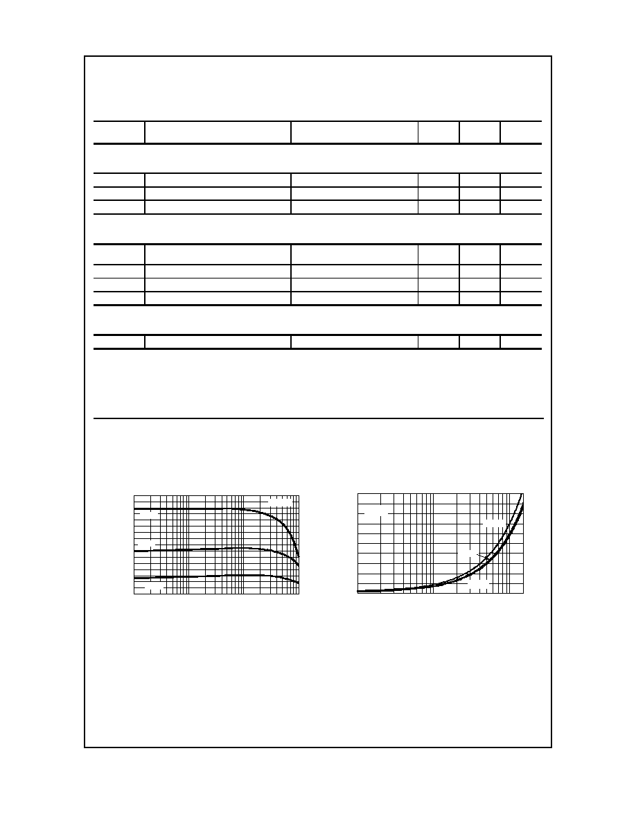
DC Typical Characteristics
Collector-Emitter Saturation
Voltage vs Collector Current
P Q
0.1
1
10 15
0
0.2
0.4
0.6
0.8
1
I - COLLECTOR CURRENT (A)
V
-
C
O
LLE
C
T
O
R
-
E
M
I
TTE
R
V
O
L
T
A
G
E
(
V
)
CE
S
A
T
C
= 10
125 ∫C
- 40 ∫C
25 ∞C
Typical Pulsed Current Gain
vs Collector Current
0.01 0.02
0.05 0.1
0.2
0.5
1
2
5
10
40
60
80
100
120
140
160
180
200
I - COLLECTOR CURRENT (A)
h
-
T
Y
P
I
CA
L
P
U
L
S
E
D
CU
RRE
NT
G
A
I
N
C
FE
125 ∞C
25 ∞C
- 40 ∞C
Vce = 5V
PNP Power Amplifier
(continued)

D45H8 / NZT45H8
DC Typical Characteristics
(continued)
Base-Emitter Saturation
Voltage vs Collector Current
0.1
1
10
0.4
0.6
0.8
1
1.2
1.4
1.6
I - COLLECTOR CURRENT (A)
V
-
B
A
SE-
EM
IT
T
E
R
VO
L
T
A
G
E
(
V
)
B
ESA
T
C
= 10
125 ∫C
- 40 ∫C
25 ∞C
Base-Emitter ON Voltage vs
Collector Current
0.1
1
10
0.4
0.6
0.8
1
1.2
1.4
I - COLLECTOR CURRENT (A)
V
-
B
A
SE-
EM
IT
T
E
R
O
N
VO
L
T
A
G
E
(
V
)
B
E(O
N
)
125 ∫C
- 40 ∫C
25 ∞C
C
V = 5V
CE
Collector-Cutoff Current
vs Ambient Temperature
P 5Q
25
50
75
100
125
150
0.01
0.1
1
10
100
T - AMBIENT TEMPERATURE ( C)
I
- CO
L
L
E
C
T
O
R
CU
RRE
N
T
(
n
A)
A
V = 50V
CB
∫
CBO
AC Typical Characteristics
PNP Power Amplifier
(continued)
Safe Operating Area TO-220

D45H8 / NZT45H8
AC Typical Characteristics
(continued)
POWER DISSIPATION vs
AMBIENT TEMPERATURE
0
25
50
75
100
125
150
0
0.25
0.5
0.75
1
1.25
1.5
TEMPERATURE ( C)
P
-
P
O
W
E
R
D
I
SS
IP
A
T
IO
N
(
W
)
D
o
SOT-223
Maximum Power Dissipation
vs. Case Temperature
Maximum Power Dissipation
vs. Ambient Temperature
Thermal Response in TO-220 Package
PNP Power Amplifier
(continued)