
© 2000 Fairchild Semiconductor Corporation
DS010620
www.fairchildsemi.com
November 1989
Revised February 2000
DM74ALS125
Quad 3
-
ST
A
T
E Buf
f
er
DM74ALS125
Quad 3-STATE Buffer
General Description
This device contains four independent gates each of which
performs a non-inverting buffer function. The outputs have
the 3-STATE feature. The 3-STATE circuitry contains a fea-
ture that maintains the buffer outputs in 3-STATE (high
impedance state) during power supply ramp-up or ramp-
down. This eliminates bus glitching problems that arise
during power-up and power-down. To minimize the possi-
bility that two outputs will attempt to take a common bus to
opposite logic levels, the disable time is shorter than the
enable time of the outputs.
Features
s
Advanced low power oxide-isolated ion-implanted
Schottky TTL process
s
Functional and pin compatible with the 74LS counterpart
s
Switching response specified into 500
and 50 pF load
s
Switching response specifications guaranteed over full
temperature and V
CC
supply range
s
PNP input design reduces input loading
s
Low level drive current: 74ALS
=
24 mA
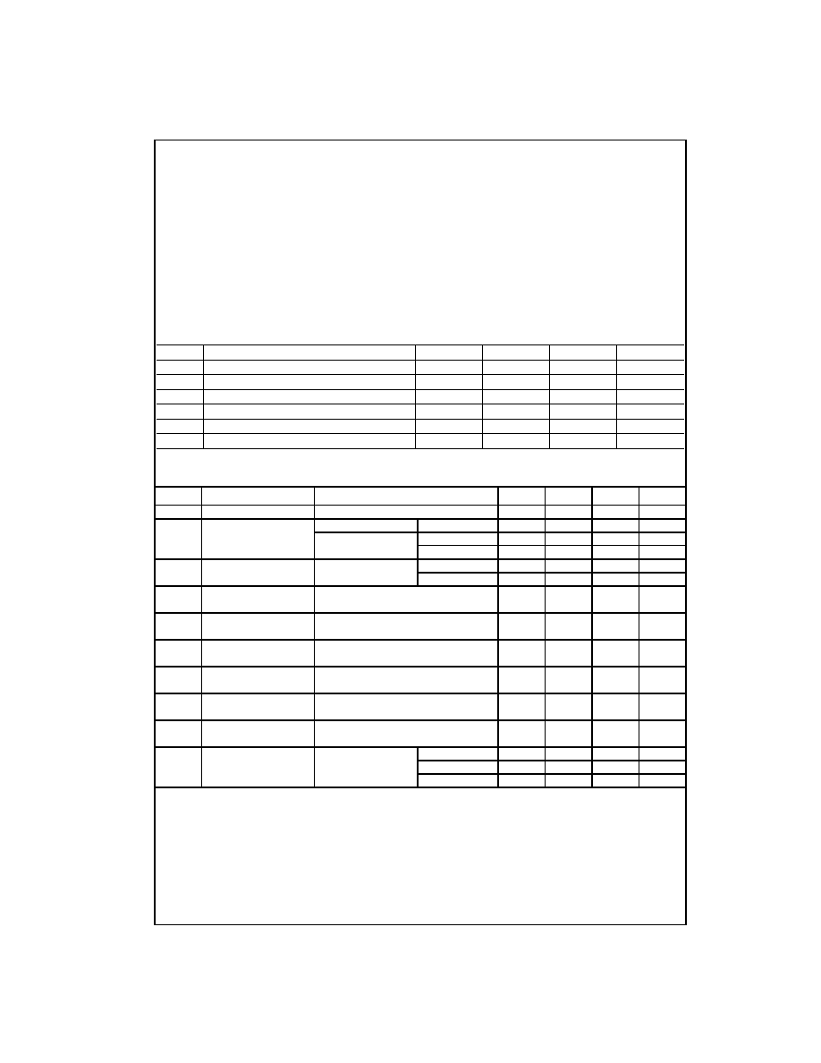
Ordering Code:
Devices also available in Tape and Reel. Specify by appending the suffix letter "X" to the ordering code.
Connection Diagram
Functional Table
Y
=
A
H
=
HIGH Logic Level
L
=
LOW Logic Level
X
=
Either LOW or HIGH Logic Level
Hi-Z
=
3-STATE (Outputs are disabled)
Logic Diagram
Order Number
Package Number
Package Description
DM74ALS125M
M14A
14-Lead Small Outline Integrated Circuit (SOIC), JEDEC MS-012, 0.150 Narrow
DM74ALS125N
N14A
14-Lead Plastic Dual-In-Line Package (PDIP), JEDEC MS-001, 0.300 Wide
Input
Output
A
C
Y
L
L
L
H
L
H
X
H
Hi-Z
www.fairchildsemi.com
2
D
M
74ALS125
Absolute Maximum Ratings
(Note 1)
Note 1: The Absolute Maximum Ratings are those values beyond which
the safety of the device cannot be guaranteed. The device should not be
operated at these limits. The parametric values defined in the Electrical
Characteristics tables are not guaranteed at the absolute maximum ratings.
The "Recommended Operating Conditions" table will define the conditions
for actual device operation.
Recommended Operating Conditions
Electrical Characteristics
over recommended operating free air temperature (unless otherwise specified)
Supply Voltage, V
CC
7V
Input Voltage
7V
Voltage Applied to Disabled Output
5.5V
Operating Free Air Temperature Range
0 to
+
70
∞
C
Storage Temperature Range
-
65
∞
C to
+
150
∞
C
Typical
JA
N Package
78.0
∞
C/W
M Package
111.0
∞
C/W
Symbol
Parameter
Min
Typ
Max
Units
V
CC
Supply Voltage
4.5
5
5.5
V
V
IH
HIGH Level Input Voltage
2
V
V
IL
LOW Level Input Voltage
0.8
V
I
OH
HIGH Level Output Current
-
15
mA
I
OL
LOW Level Output Current
24
mA
T
A
Operating Free-Air Temperature
0
70
∞
C
Symbol
Parameter
Conditions
Min
Typ
Max
Units
V
IK
Input Clamp Voltage
V
CC
=
4.5V, I
I
=
-
18 mA
-
1.5
V
V
OH
HIGH Level
V
CC
=
4.5V to 5.5V
I
OH
=
-
0.4 mA
V
CC
-
2
V
Output Voltage
V
CC
=
4.5V
I
OH
=
-
3 mA
2.4
V
I
OH
=
Max
2
V
V
OL
LOW Level
V
CC
=
4.5V
I
OL
=
12 mA
0.25
0.4
V
Output Voltage
I
OL
=
24 mA
0.35
0.5
V
I
I
Input Current at Max
V
CC
=
5.5V, V
I
=
7V
0.1
mA
Input Voltage
I
IH
HIGH Level
V
CC
=
5.5V, V
I
=
2.7V
20
µ
A
Input Current
I
IL
LOW Level
V
CC
=
5.5V, V
IL
=
0.4V
-
0.1
mA
Input Current
I
O
Output Drive
V
CC
=
5.5V, V
O
=
2.25V
-
30
-
112
mA
Current
I
OZH
HIGH Level 3-STATE
V
CC
=
5.5V, V
O
=
2.7V
20
µ
A
Output Current
I
OZL
LOW Level 3-STATE
V
CC
=
5.5V, V
O
=
0.4V
-
20
µ
A
Output Current
I
CC
Supply Current
V
CC
=
5.5V
Outputs HIGH
7
10
mA
Outputs LOW
10
14
mA
3-STATE
13.5
18
mA

3
www.fairchildsemi.com
DM74ALS125
Switching Characteristics
Symbol
Parameter
From
To
Conditions
Min
Max
Units
(Input)
(Output)
t
PLH
Propagation Delay Time
A
Y
V
CC
=
4.5V to 5.5V,
3
10
ns
LOW-to-HIGH Level Output
C
L
=
50 pF,
t
PHL
Propagation Delay Time
A
Y
R1
=
500
,
2
10
ns
HIGH-to-LOW Level Output
R2
=
500
,
t
PZH
Output Enable Time
C
Y
T
A
=
Min to Max
2
13
ns
to HIGH Level Output
t
PZL
Output Enable Time
C
Y
2
12
ns
to LOW Level Output
t
PHZ
Output Disable Time
C
Y
1
8
ns
from HIGH Level Output
t
PLZ
Output Disable Time
C
Y
2
13
ns
from LOW Level Output

www.fairchildsemi.com
4
D
M
74ALS125
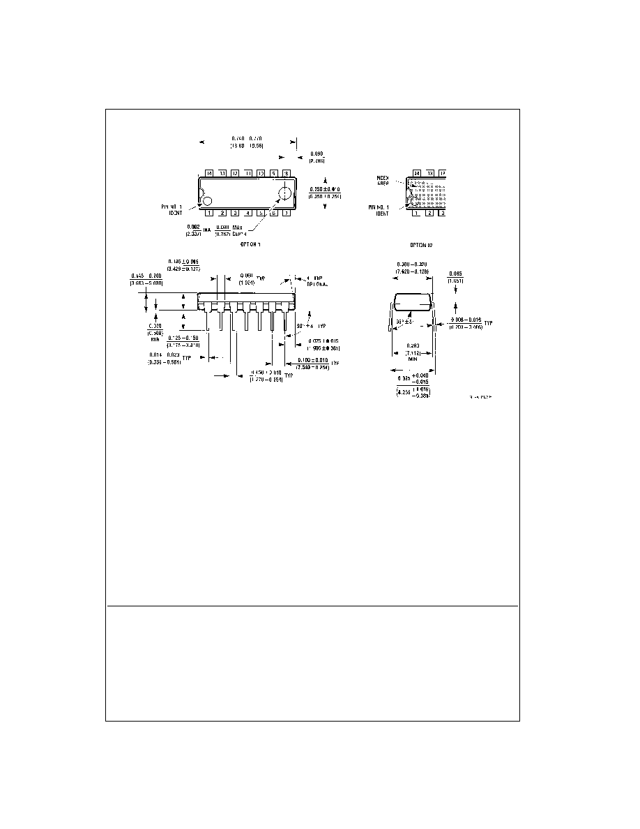
Physical Dimensions
inches (millimeters) unless otherwise noted
14-Lead Small Outline Integrated Circuit (SOIC), JEDEC MS-012, 0.150 Narrow
Package Number M14A
5
www.fairchildsemi.com
DM74ALS125
Quad 3
-
ST
A
T
E Buf
f
er
Physical Dimensions
inches (millimeters) unless otherwise noted (Continued)
14-Lead Plastic Dual-In-Line Package (PDIP), JEDEC MS-001, 0.300 Wide
Package Number N14A
Fairchild does not assume any responsibility for use of any circuitry described, no circuit patent licenses are implied and
Fairchild reserves the right at any time without notice to change said circuitry and specifications.
LIFE SUPPORT POLICY
FAIRCHILD'S PRODUCTS ARE NOT AUTHORIZED FOR USE AS CRITICAL COMPONENTS IN LIFE SUPPORT
DEVICES OR SYSTEMS WITHOUT THE EXPRESS WRITTEN APPROVAL OF THE PRESIDENT OF FAIRCHILD
SEMICONDUCTOR CORPORATION. As used herein:
1. Life support devices or systems are devices or systems
which, (a) are intended for surgical implant into the
body, or (b) support or sustain life, and (c) whose failure
to perform when properly used in accordance with
instructions for use provided in the labeling, can be rea-
sonably expected to result in a significant injury to the
user.
2. A critical component in any component of a life support
device or system whose failure to perform can be rea-
sonably expected to cause the failure of the life support
device or system, or to affect its safety or effectiveness.
www.fairchildsemi.com