
© 2000 Fairchild Semiconductor Corporation
DS006204
www.fairchildsemi.com
April 1984
Revised February 2000
DM74ALS153 Dual
1-
of-
4
L
i
ne Data Sele
ctor
/Mul
ti
plexer
DM74ALS153
Dual 1-of-4 Line Data Selector/Multiplexer
General Description
This Data Selector/Multiplexer contains full on-chip decod-
ing to select one-of-four data sources as a result of a
unique two-bit binary code at the Select inputs. Each of the
two Data Selector/Multiplexer circuits have their own sepa-
rate Data and Strobe inputs and a non-inverting output
buffer. The Select inputs A and B are common to both sec-
tions. The Strobe inputs, when at the HIGH level, disable
their associated data inputs and force the corresponding
output to the LOW state. The Select input buffers incorpo-
rate internal overlap features to ensure that select input
changes do not cause invalid output transients.
Features
s
Advanced oxide-isolated, ion-implanted Schottky TTL
process
s
Switching performance is guaranteed over full tempera-
ture and V
CC
supply range
s
Pin and functional compatible with LS family counterpart
s
Improved output transient handling capability
Ordering Code:
Devices also available in Tape and Reel. Specify by appending the suffix letter "X" to the ordering code.
Connection Diagram
Function Table
Select inputs A and B are common to both sections.
H
=
HIGH Level
L
=
LOW Level
X
=
Don't Care
Order Number
Package Number
Package Description
DM74ALS153M
M16A
16-Lead Small Outline Integrated Circuit (SOIC), JEDEC MS-012, 0.150 Narrow
DM74ALS153SJ
M16D
16-Lead Small Outline Package (SOP), EIAJ TYPE II, 5.3mm Wide
DM74ALS153N
N16E
16-Lead Plastic Dual-In-Line Package (PDIP), JEDEC MS-001, 0.300 Wide
Select
Data Inputs
Strobe
Output
Inputs
B
A
C0
C1
C2
C3
G
Y
X
X
X
X
X
X
H
L
L
L
L
X
X
X
L
L
L
L
H
X
X
X
L
H
L
H
X
L
X
X
L
L
L
H
X
H
X
X
L
H
H
L
X
X
L
X
L
L
H
L
X
X
H
X
L
H
H
H
X
X
X
L
L
L
H
H
X
X
X
H
L
H

3
www.fairchildsemi.com
DM74ALS153
Absolute Maximum Ratings
(Note 1)
Note 1: The "Absolute Maximum Ratings" are those values beyond which
the safety of the device cannot be guaranteed. The device should not be
operated at these limits. The parametric values defined in the Electrical
Characteristics tables are not guaranteed at the absolute maximum ratings.
The "Recommended Operating Conditions" table will define the conditions
for actual device operation.
Recommended Operating Conditions
Electrical Characteristics
over recommended operating free air temperature range. All typical values are measured at V
CC
=
5V, T
A
=
25
∞
C.
Switching Characteristics
over recommended operating free air temperature range.
Supply Voltage
7V
Input Voltage
7V
Operating Free Air Temperature Range
0
∞
C to
+
70
∞
C
Storage Temperature Range
-
65
∞
C to
+
150
∞
C
Typical
JA
N Package
78.0
∞
C/W
M Package
107.0
∞
C/W
Symbol
Parameter
Min
Nom
Max
Units
V
CC
Supply Voltage
4.5
5
5.5
V
V
IH
HIGH Level Input Voltage
2
V
V
IL
LOW Level Input Voltage
0.8
V
I
OH
HIGH Level Output Current
-
2.6
mA
I
OL
LOW Level Output Current
24
mA
T
A
Free Air Operating Temperature
0
70
∞
C
Symbol
Parameter
Conditions
Min
Typ
Max
Units
V
IK
Input Clamp Voltage
V
CC
=
4.5V, I
IN
=
-
18 mA
-
1.5
V
V
OH
HIGH Level
V
CC
=
4.5V, I
OH
=
Max
2.4
3.2
V
Output Voltage
I
OH
=
-
400
µ
A, V
CC
=
4.5V to 5.5V
V
CC
-
2
V
V
OL
LOW Level
V
CC
=
4.5V
I
OL
=
24 mA
0.35
0.5
V
Output Voltage
I
I
Input Current at
V
CC
=
5.5V, V
IN
=
7V
0.1
mA
Max Input Voltage
I
IH
High Level Input Current
V
CC
=
5.5V, V
IN
=
2.7V
20
µ
A
I
IL
Low Level Input Current
V
CC
=
5.5V, V
IN
=
0.4V
-
0.1
mA
I
O
Output Drive Current
V
CC
=
5.5V, V
OUT
=
2.25V
-
30
-
112
mA
I
CC
Supply Current
V
CC
=
5.5V
7.5
14
mA
All Inputs
=
4.5V
Symbol
Parameter
Conditions
From
To
Min
Max
Units
t
PLH
Propagation Delay Time
V
CC
=
4.5V to 5.5V
Select
Y
5
21
ns
LOW-to-HIGH Level Output
C
L
=
50 pF
t
PHL
Propagation Delay Time
R
L
=
500
Select
Y
5
21
ns
HIGH-to-LOW Level Output
t
PLH
Propagation Delay Time
Data
Y
3
10
ns
LOW-to-HIGH Level Output
t
PHL
Propagation Delay Time
Data
Y
4
15
ns
HIGH-to-LOW Level Output
t
PLH
Propagation Delay Time
Strobe
Y
5
18
ns
LOW-to-HIGH Level Output
t
PHL
Propagation Delay Time
Strobe
Y
5
18
ns
HIGH-to-LOW Level Output
www.fairchildsemi.com
4
D
M
74ALS153
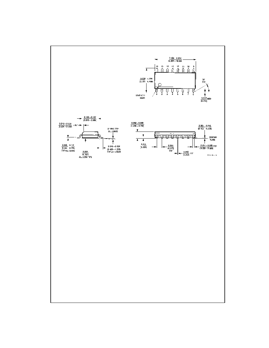
Physical Dimensions
inches (millimeters) unless otherwise noted
16-Lead Small Outline Integrated Circuit (SOIC), JEDEC MS-012, 0.150 Narrow
Package Number M16A
5
www.fairchildsemi.com
DM74ALS153
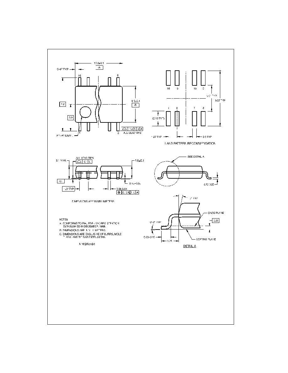
Physical Dimensions
inches (millimeters) unless otherwise noted (Continued)
16-Lead Small Outline Package (SOP), EIAJ TYPE II, 5.3mm Wide
Package Number M16D
