© 2000 Fairchild Semiconductor Corporation
DS006212
www.fairchildsemi.com
September 1986
Revised February 2000
DM74ALS244A Octal
3
-
ST
A
T
E
Bus Driv
er
DM74ALS244A
Octal 3-STATE Bus Driver
General Description
This octal 3-STATE bus driver is designed to provide the
designer with flexibility in implementing a bus interface with
memory, microprocessor, or communication systems. This
device offers 64-extended temperature Grade product
guaranteeing performance from
-
40
∞
C to
+
85
∞
C. The out-
put 3-STATE gating control is organized into two separate
groups of four buffers, and both control inputs enable the
respective outputs when set logic LOW. The 3-STATE cir-
cuitry contains a feature that maintains the buffer outputs in
3-STATE (high impedance state) during power supply
ramp-up or ramp-down. This eliminates bus glitching prob-
lems that arise during power-up and power-down.
Features
s
Advanced low power oxide-isolated ion-implanted
Schottky TTL process
s
Functional and pin compatible with the 74LS counterpart
s
Improved switching performance with less power dissi-
pation compared with the 74LS counterpart
s
Switching response specified into 500
and 50 pF load
s
Switching response specifications guaranteed over full
temperature and V
CC
supply range
s
PNP input design reduces input loading
Ordering Code:
Devices also available in Tape and Reel. Specify by appending the suffix letter "X" to the ordering code.
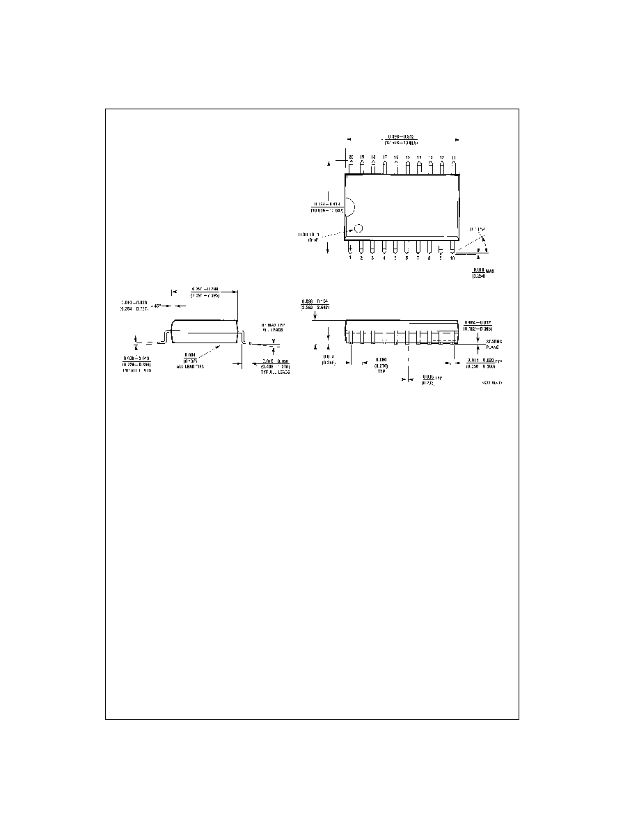
Connection Diagram
Function Table
H
=
HIGH Level Logic State
L
=
LOW Level Logic State
X
=
Don't Care (Either LOW or HIGH Level Logic State)
Z
=
High Impedance (OFF) State
Logic Diagram
Order Number
Package Number
Package Description
DM74ALS244AWM
M20B
20-Lead Small Outline Integrated Circuit (SOIC), JEDEC MS-013, 0.300 Wide
DM74ALS244ASJ
M20D
20-Lead Small Outline Package (SOP), EIAJ TYPE II, 5.3mm Wide
DM74ALS244AMSA
MSA20
20-Lead Shrink Small Outline Package (SSOP), EIAJ TYPE II, 5.3mm Wide
DM74ALS244AN
N20A
20-Lead Plastic Dual-In-Line Package (PDIP), JEDEC MS-001, 0.300 Wide
Input
Output
G
A
Y
L
L
L
L
H
H
H
X
Z

www.fairchildsemi.com
2
DM
74ALS24
4A
Absolute Maximum Ratings
(Note 1)
Note 1: The "Absolute Maximum Ratings" are those values beyond which
the safety of the device cannot be guaranteed. The device should not be
operated at these limits. The parametric values defined in the Electrical
Characteristics tables are not guaranteed at the absolute maximum ratings.
The "Recommended Operating Conditions" table will define the conditions
for actual device operation.
Recommended Operating Conditions
Electrical Characteristics
over recommended operating free air temperature (unless otherwise specified)
Switching Characteristics
over recommended operating free-air temperature range
Supply Voltage, V
CC
7V
Input Voltage
7V
Voltage Applied to Disabled Output
5.5V
Operating Free Air Temperature Range
0
∞
C to
+
70
∞
C
Storage Temperature Range
-
65
∞
C to
+
150
∞
C
Typical
JA
N Package
60.5
∞
C/W
M Package
79.8
∞
C/W
Symbol
Parameter
Min
Typ
Max
Units
V
CC
Supply Voltage
4.5
5
5.5
V
V
IH
HIGH Level Input Voltage
2
V
V
IL
LOW Level Input Voltage
0.8
V
I
OH
HIGH Level Output Current
-
15
mA
I
OL
LOW Level Output Current
24
mA
T
A
Operating Free-Air Temperature
0
70
∞
C
Symbol
Parameter
Conditions
Min
Typ
Max
Units
V
IK
Input Clamp Voltage
V
CC
=
4.5V, I
I
=
-
18 mA
-
1.5
V
V
OH
HIGH Level
V
CC
=
4.5V to 5.5V
I
OH
=
-
0.4 mA
V
CC
-
2
V
Output Voltage
V
CC
=
4.5V
I
OH
=
-
3 mA
2.4
V
I
OH
=
Max
2
V
V
OL
LOW
Level V
CC
=
4.5V
0.35
0.5
V
Output Voltage
I
OL
=
24 mA
I
I
Input Current at Maximum Input Voltage V
CC
=
5.5V, V
I
=
7V
0.1
mA
I
IH
HIGH Level Input Current
V
CC
=
5.5V, V
I
=
2.7V
20
µ
A
I
IL
LOW Level Input Current
V
CC
=
5.5V, V
IL
=
0.4V
-
0.1
mA
I
O
Output Drive Current
V
CC
=
5.5V, V
O
=
2.25V
-
30
-
112
mA
I
OZH
HIGH Level 3-STATE Output Current
V
CC
=
5.5V, V
O
=
2.7V
20
µ
A
I
OZL
LOW Level 3-STATE Output Current
V
CC
=
5.5V, V
O
=
0.4V
-
20
µ
A
I
CC
Supply Current
V
CC
=
5.5V
9
15
mA
Outputs HIGH
Outputs LOW
15
24
mA
Outputs 3-STATE
17
27
mA
Symbol
Parameter
Conditions
From
(Input)
To
(Output)
Min
Max
Units
t
PLH
Propagation Delay Time
V
CC
=
4.5V to 5.5V,
A
Y
3
10
ns
LOW-to-HIGH Level Output
C
L
=
50 pF,
t
PHL
Propagation Delay Time
R1
=
500
,
A
Y
3
10
ns
HIGH-to-LOW Level Output
R2
=
500
,
t
PZH
Output Enable Time to HIGH Level Output
T
A
=
Min to Max
G
Y
3
20
ns
t
PZL
Output Enable Time to LOW Level Output
G
Y
3
20
ns
t
PHZ
Output Disable Time from HIGH Level Output
G
Y
2
10
ns
t
PLZ
Output Disable Time from LOW Level Output
G
Y
1
13
ns