© 2000 Fairchild Semiconductor Corporation
DS006216
www.fairchildsemi.com
April 1984
Revised February 2000
DM74ALS273 Octal
D
-
T
ype Edge-T
r
igger
ed Fli
p
-Fl
op w
i
th Cle
a
r
DM74ALS273
Octal D-Type Edge-Triggered Flip-Flop with Clear
General Description
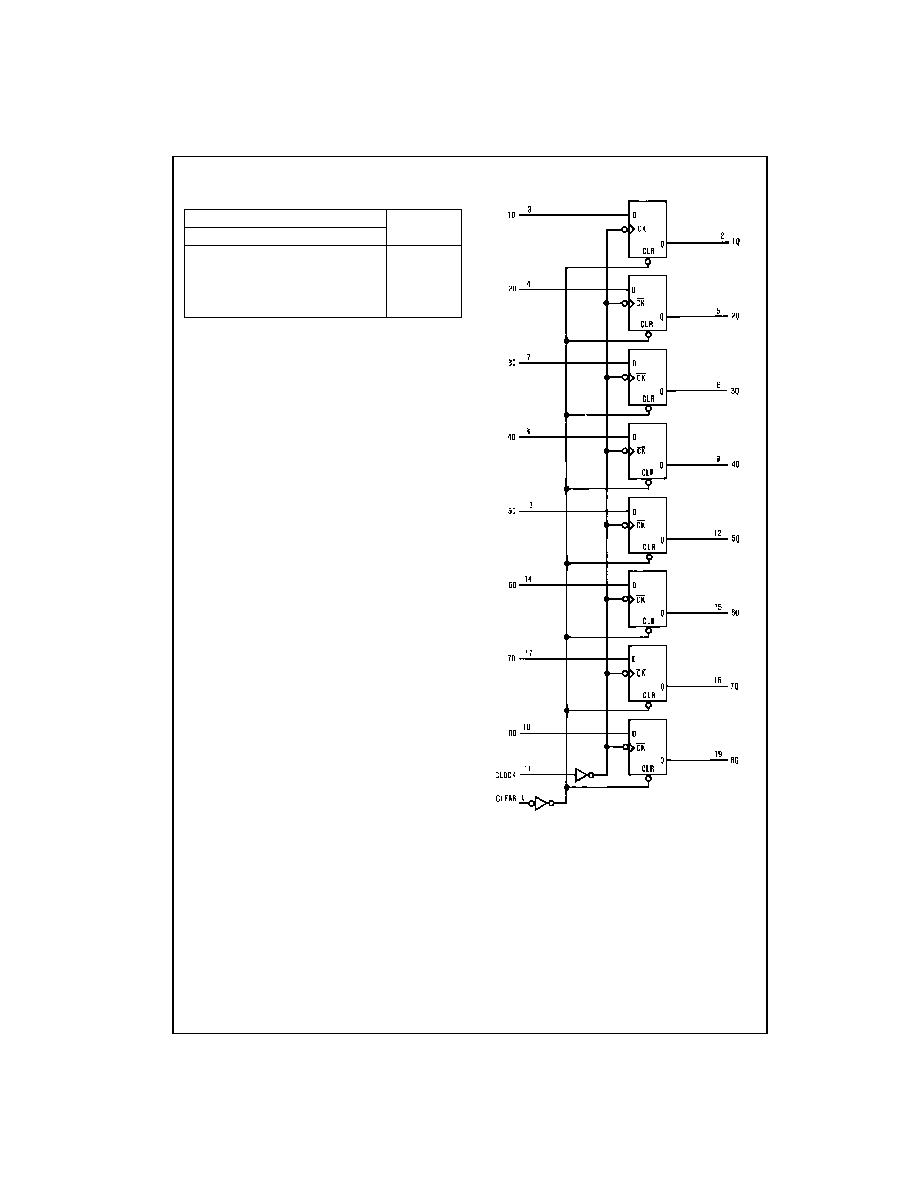
These monolithic, positive-edge-triggered flip-flops utilize
TTL circuitry to implement D-type flip-flop logic with a direct
clear input.
Information at the D inputs meeting the setup requirements
is transferred to the Q outputs on the positive-going edge
of the clock pulse. Clock triggering occurs at a particular
voltage level and is not directly related to the transition time
of the positive-going pulse. When the clock input is at
either the HIGH or LOW level, the D input signal has no
effect at the output.
Features
s
Switching specifications at 50 pF
s
Switching specifications guaranteed over full tempera-
ture and V
CC
range
s
Buffer-type outputs and improved AC offer significant
advantage over DM74LS273.
s
Advanced oxide-isolated, ion-implanted Schottky TTL
process
s
Functionally and pin-for-pin compatible with
DM74LS273.
Ordering Code:
Devices also available in Tape and Reel. Specify by appending the suffix letter "X" to the ordering code.
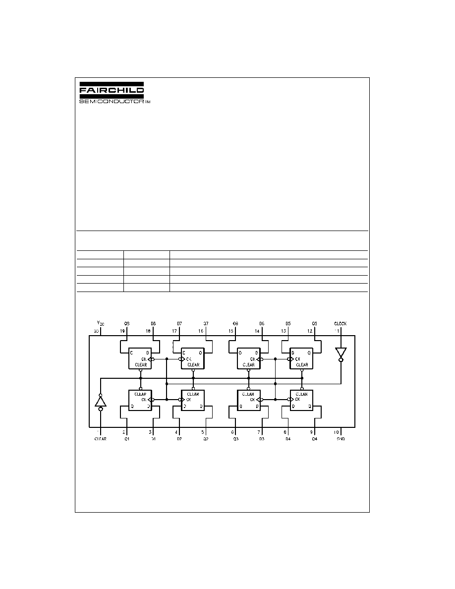
Connection Diagram
Order Number
Package Number
Package Description
DM74ALS273WM
M20B
20-Lead Small Outline Integrated Circuit (SOIC), JEDEC MS-013, 0.300 Wide
DM74ALS273SJ
M20D
20-Lead Small Outline Package (SOP), EIAJ TYPE II, 5.3mm Wide
DM74ALS273MSA
MSA20
20-Lead Shrink Small Outline Package (SSOP), EIAJ TYPE II, 5.3mm Wide
DM74ALS273N
N20A
20-Lead Plastic Dual-In-Line Package (PDIP), JEDEC MS-001, 0.300 Wide

3
www.fairchildsemi.com
DM74ALS273
Absolute Maximum Ratings
(Note 1)
Note 1: The "Absolute Maximum Ratings" are those values beyond which
the safety of the device cannot be guaranteed. The device should not be
operated at these limits. The parametric values defined in the Electrical
Characteristics tables are not guaranteed at the absolute maximum ratings.
The "Recommended Operating Conditions" table will define the conditions
for actual device operation.
Recommended Operating Conditions
Note 2: The (
) arrow indicates the positive edge of the Clock is used for reference.
Electrical Characteristics
over recommended operating free air temperature range. All typical values are measured at V
CC
=
5V, T
A
=
25
∞
C.
Switching Characteristics
over recommended operating free air temperature range.
Supply Voltage
7V
Input Voltage
7V
Operating Free Air Temperature Range
0
∞
C to
+
70
∞
C
Storage Temperature Range
-
65
∞
C to
+
150
∞
C
Typical
JA
N Package
60.0
∞
C/W
M Package
79.0
∞
C/W
Symbol
Parameter
Min
Nom
Max
Units
V
CC
Supply Voltage
4.5
5
5.5
V
V
IH
HIGH Level Input Voltage
2
V
V
IL
LOW Level Input Voltage
0.8
V
I
OH
HIGH Level Output Current
-
2.6
mA
I
OL
LOW Level Output Current
24
mA
f
CLK
Clock Frequency
0
35
MHz
t
W(CLK)
Width of Clock Pulse
HIGH
14
ns
LOW
14
ns
t
W
Width of Clear Pulse
LOW
10
ns
t
SU
Data Setup Time (Note 2)
10
ns
Clear Inactive
15
t
H
Data Hold Time
0
ns
T
A
Free Air Operating Temperature
0
70
∞
C
Symbol
Parameter
Conditions
Min
Typ
Max
Units
V
IK
Input Clamp Voltage
V
CC
=
4.5V, I
I
=
-
18 mA
-
1.5
V
V
OH
HIGH Level
V
CC
=
4.5V
I
OH
=
-
2.6 mA
2.4
3.3
V
Output Voltage
V
CC
=
4.5V to 5.5V
I
OH
=
-
400
µ
A
V
CC
-
2
V
V
OL
LOW Level
V
CC
=
4.5V
I
OL
=
12 mA
0.25
0.4
V
Output Voltage
I
OL
=
24 mA
0.35
0.5
V
I
I
Input Current @ Maximum Input Voltage V
CC
=
5.5V, V
IH
=
7V
0.1
mA
I
IH
HIGH Level Input Current
V
CC
=
5.5V, V
IH
=
2.7V
20
µ
A
I
IL
LOW Level Input Current
V
CC
=
5.5V, V
IL
=
0.4V
-
0.2
mA
I
O
Output Drive Current
V
CC
=
5.5V
V
O
=
2.25V
-
30
-
112
mA
I
CC
Supply Current
V
CC
=
5.5V
Outputs HIGH
11
20
mA
Outputs OPEN
Outputs LOW
19
29
mA
Symbol
Parameter
Conditions
From
To
Min
Max
Units
f
MAX
Maximum Clock Frequency
V
CC
=
4.5V to 5.5V
35
MHz
t
PHL
Propagation Delay Time
R
L
=
500
Clear
Any Q
4
18
ns
HIGH-to-LOW Level Output
C
L
=
50 pF
t
PLH
Propagation Delay Time
Clock
Any Q
2
12
ns
LOW-to-HIGH Level Output
t
PHL
Propagation Delay Time
Clock
Any Q
3
15
ns
HIGH-to-LOW Level Output
www.fairchildsemi.com
4
D
M
74ALS273
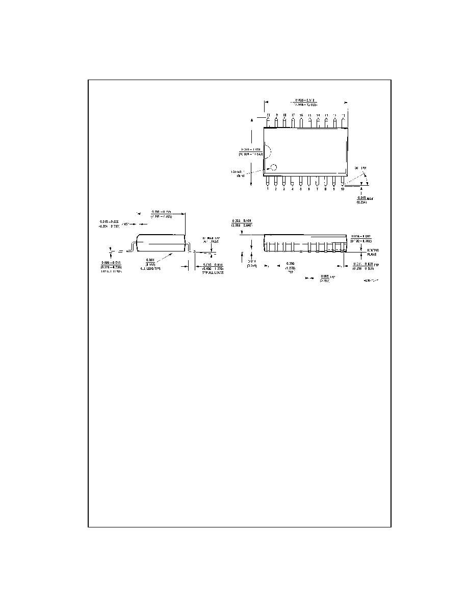
Physical Dimensions
inches (millimeters) unless otherwise noted
20-Lead Small Outline Integrated Circuit (SOIC), JEDEC MS-013, 0.300 Wide
Package Number M20B

5
www.fairchildsemi.com
DM74ALS273
Physical Dimensions
inches (millimeters) unless otherwise noted (Continued)
20-Lead Small Outline Package (SOP), EIAJ TYPE II, 5.3mm Wide
Package Number M20D