© 2000 Fairchild Semiconductor Corporation
DS009175
www.fairchildsemi.com
October 1986
Revised February 2000
DM74ALS5245
Octa
l
3-ST
A
T
E T
r
anscei
ver
DM74ALS5245
Octal 3-STATE Transceiver
General Description
This octal bus transceiver is designed for asynchronous
two-way communication between data buses. The inputs
include hysteresis which provides improved noise rejec-
tion. Data is transmitted either from the A bus to the B bus
or from the B bus to the A bus depending on the logic level
of the direction control (DIR) input. The device can be dis-
abled via the enable input (G) which causes the outputs to
enter the high impedance mode so the buses are effec-
tively isolated.
Features
s
Input Hysteresis
s
Low output noise generation
s
High input noise immunity
s
Advanced oxide-isolated, ion implanted Schottky TTL
process
s
Switching specification guaranteed over the full temper-
ature and V
CC
range
s
PNP inputs to reduce input loading
Ordering Code:
Devices also available in Tape and Reel. Specify by appending the suffix letter "X" to the ordering code.
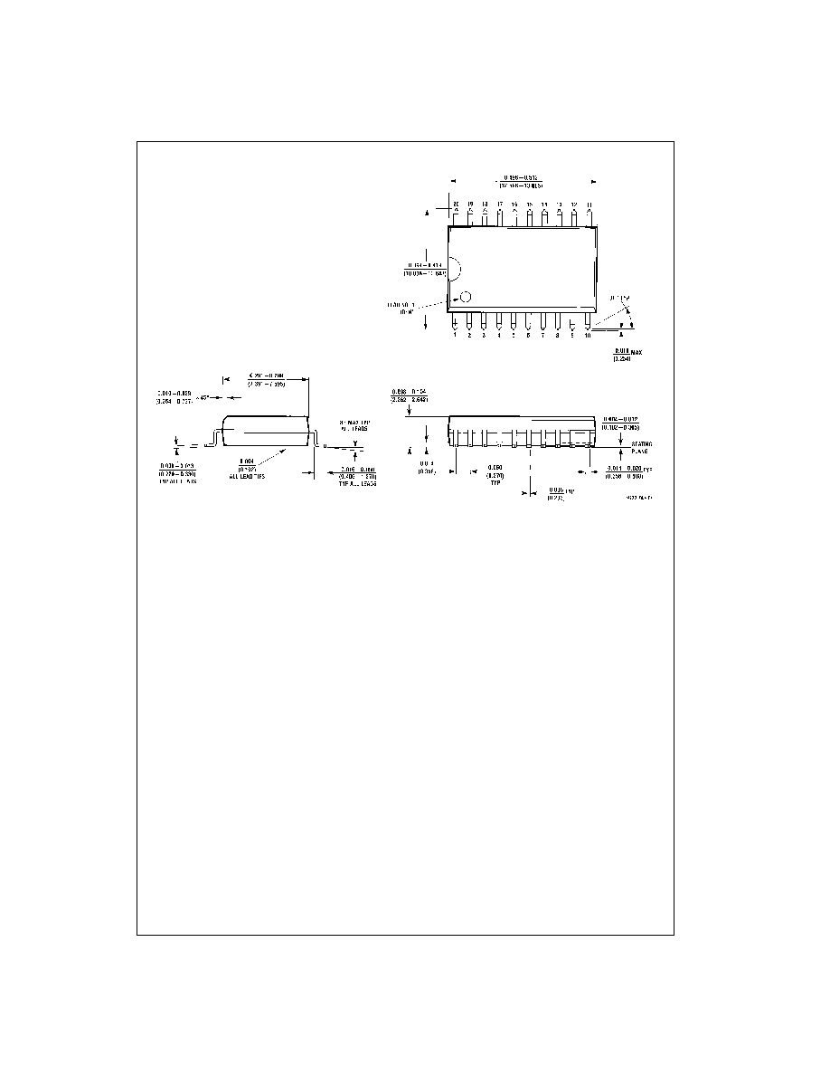
Connection Diagram
Function Table
L
=
LOW Logic Level
H
=
HIGH Logic Level
X
=
Don't Care (Either LOW or HIGH Logic Level)
Order Number
Package Number
Package Description
DM74ALS5245WM
M20B
20-Lead Small Outline Integrated Circuit (SOIC), JEDEC MS-013, 0.300 Wide
DM74ALS5245SJ
M20D
20-Lead Small Outline Package (SOP), EIAJ TYPE II, 5.3mm Wide
DM74ALS5245N
N20A
20-Lead Plastic Dual-In-Line Package (PDIP), JEDEC MS-001, 0.300 Wide
Control Inputs
Operation
G
DIR
L
L
B Data to A Bus
L
H
A Data to B Bus
H
X
High Impedance

www.fairchildsemi.com
2
DM74ALS5245
Absolute Maximum Ratings
(Note 1)
Note 1: The "Absolute Maximum Ratings" are those values beyond which
the safety of the device cannot be guaranteed. The device should not be
operated at these limits. The parametric values defined in the Electrical
Characteristic tables are not guaranteed at the absolute maximum ratings.
The "Recommended Operating Conditions" table will define the conditions
for actual device operation.
Recommended Operating Conditions
Electrical Characteristics
over recommended free air temperature range. All typical values are measured at V
CC
=
5V, T
A
=
25
∞
C.
Note 2: Plastic DIP package.
Note 3: n
=
number of device outputs; n
-
1 outputs switching, each driven 0V to 3V one output @ GND.
Note 4: n
=
number of device outputs; n outputs switching, n
-
1 inputs switching 0V to 3V. Input under test switching 3V to threshold (V
ILD
); 0V to threshold
(V
IHD
); f
=
1 MHz.
Supply Voltage
7V
Input Voltage
Control Inputs
7V
I/O Ports
5.5V
Operating Free-Air Temperature Range
0
∞
C to
+
70
∞
C
Storage Temperature Range
-
65
∞
C to
+
150
∞
C
Typical
JA
N Package
56.0
∞
C/W
M Package
74.0
∞
C/W
Symbol
Parameter
Min
Max
Units
V
CC
Supply Voltage
4.5
5.5
V
V
IH
HIGH Level Input Voltage
2
V
V
IL
LOW Level Input Voltage
0.8
V
I
OH
HIGH Level Output Current
-
15
mA
I
OL
LOW Level Output Current
24
mA
T
A
Free Air Operating Temperature Range
0
70
∞
C
Symbol
Parameter
Test Conditions
Min
Typ
Max
Units
V
IK
Input Clamp Voltage
V
CC
=
Min, I
I
=
-
18 mA
-
1.5
V
H
YS
Hysteresis (V
T
+
-
V
T
-
)
V
CC
=
Min
0.2
0.32
V
V
OH
HIGH Level
V
CC
=
4.5V to 5.5V
I
OH
=
-
0.4 mA
V
CC
-
2
Output Voltage
V
CC
=
Min
I
OH
=
-
3 mA
2.4
3.2
V
I
OH
=
Max
2
V
OL
LOW
Level V
CC
=
Min
I
OL
=
12 mA
0.25
0.4
V
Output Voltage
I
OL
=
24 mA
0.35
0.5
I
I
Input Current at
V
CC
=
Max
I/O Ports, V
I
=
5.5V
100
µ
A
Maximum Input Voltage
Control Inputs, V
I
=
7V
100
I
IH
HIGH Level Input Current
V
CC
=
Max, V
I
=
2.7V
20
µ
A
I
IL
LOW Level Input Current
V
CC
=
Max, V
I
=
0.4V
-
100
µ
A
I
O
Output Drive Current
V
CC
=
Max, V
O
=
2.25V
-
30
-
112
mA
I
CC
Supply Current
V
CC
=
Max
Outputs HIGH
30
45
Outputs LOW
36
55
mA
Outputs Disabled
38
58
V
OLP
Quiet Output Maximum
V
CC
=
5.0V, T
A
=
25
∞
C
0.5
V
Dynamic V
OL
(Figures 1, 2; (Note 2)(Note 3))
V
OLV
Quiet Output Minimum
V
CC
=
5.0V, T
A
=
25
∞
C
-
0.2
V
Dynamic V
OL
(Figures 1, 2; (Note 2)(Note 3))
V
IHD
Minimum High Level
V
CC
=
5.0V, T
A
=
25
∞
C
1.6
V
Dynamic Input Voltage
(Note 2)(Note 4)
V
ILD
Maximum Low Level
V
CC
=
5.0V, T
A
=
25
∞
C
1.0
V
Dynamic Input Voltage
(Note 2)(Note 4)
www.fairchildsemi.com
4
DM74ALS5245
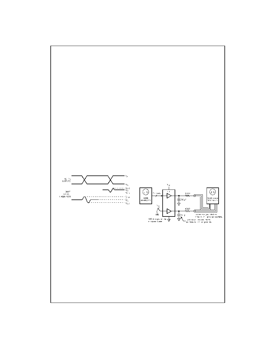
ALS Noise Characteristics
The setup of a noise characteristics measurement is critical
to the accuracy and repeatability of the tests. The following
is a brief description of the setup used to measure the
noise characteristics of ALS.
Equipment:
Word Generator
Printed Circuit Board Test Fixture
Dual Trace Oscilloscope
Procedure:
1. Verify Test Fixture Loading: Standard Load 50 pF,
500
.
2. Deskew the word generator so that no two channels
have greater than 150 ps skew between them. This
requires that the oscilloscope be deskewed first. Swap
out the channels that have more than 150 ps of skew
until all channels being used are within 150 ps. It is
important to deskew the word generator channels
before testing. This will ensure that the outputs switch
simultaneously.
3. Terminate all inputs and outputs to ensure proper load-
ing of the outputs and that the input levels are at the
correct voltage.
4. Set V
CC
to 5.0V.
5. Set the word generator to toggle all but one output at a
frequency of 1 MHz. Greater frequencies will increase
DUT heating and affect the results of the measure-
ment.
6. Set the word generator input levels at 0V LOW and 3V
HIGH. Verify levels with a digital volt meter.
FIGURE 1. Quiet Output Noise Voltage Waveforms
Note 5: V
OHV
and V
OHP
are measured with respect to V
OH
reference. V
OLV
and V
OLP
are measured with respect to ground reference.
Note 6: Input pulses have the following characteristics: f
=
1 MHz, t
r
=
3 ns,
t
f
=
3 ns, skew
<
150 ps.
V
OLP
/V
OLV
and V
OHP
/V
OHV
:
∑ Determine the quiet output pin that demonstrates the
greatest noise levels. The worst case pin will usually be
the furthest from the ground pin. Monitor the output volt-
ages using a 50
coaxial cable plugged into a standard
SMB type connector on the test fixture. Do not use an
active FET probe.
∑ Measure V
OLP
and V
OLV
on the quiet output during the
HL transition. Measure V
OHP
and V
OHV
on the quiet out-
put during the LH transition.
∑ Verify that the GND reference recorded on the oscillo-
scope has not drifted to ensure the accuracy and repeat-
ability of the measurements.
V
ILD
and V
IHD
:
∑ Monitor one of the switching outputs using a 50
coaxial
cable plugged into a standard SMB type connector on
the test fixture. Do not use an active FET probe.
∑ First increase the input LOW voltage level, V
IL
, until the
output begins to oscillate. Oscillation is defined as noise
on the output LOW level that exceeds V
IL
limits, or on
output HIGH levels that exceed V
IH
limits. The input
LOW voltage level at which oscillation occurs is defined
as V
ILD
.
∑ Next decrease the input HIGH voltage level on the word
generator, V
IH
until the output begins to oscillate. Oscil-
lation is defined as noise on the output LOW level that
exceeds V
IL
limits, or on output HIGH levels that exceed
V
IH
limits. The input HIGH voltage level at which oscilla-
tion occurs is defined as V
IHD
.
∑ Verify that the GND reference recorded on the oscillo-
scope has not drifted to ensure the accuracy and repeat-
ability of the measurements.
FIGURE 2. Simultaneous Switching Test Circuit