© 2000 Fairchild Semiconductor Corporation
DS009171
www.fairchildsemi.com
October 1986
Revised February 2000
DM74ALS541 Octal
B
u
f
f
e
r and
Li
ne Driv
er w
i
th 3-
ST
A
T
E O
u
t
put
s
DM74ALS541
Octal Buffer and Line Driver with 3-STATE Outputs
General Description
This octal buffer and line driver is designed to have the per-
formance of the DM74ALS240A series and, at the same
time, offer a pinout with inputs and outputs on opposite
sides of the package. This arrangement greatly enhances
circuit board layout. The 3-STATE control gate is a 2-input
NOR such that if either G1 or G2 is HIGH, all eight outputs
are in the high impedance state.
Features
s
Advanced oxide-isolated ion-implanted Schottky TTL
process
s
Switching performance is guaranteed over full tempera-
ture and V
CC
supply range
s
Data flow-thru pinout (all inputs on opposite side from
outputs)
s
P-N-P Inputs reduce DC loading
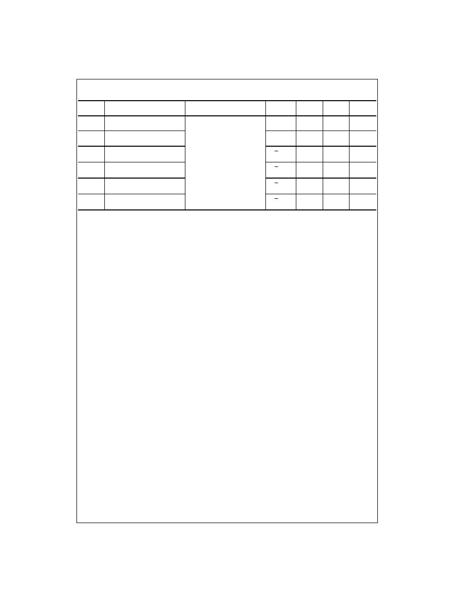
Ordering Code:
Devices also available in Tape and Reel. Specify by appending the suffix letter "X" to the ordering code.
Connection Diagram
Function Table
H
=
HIGH Logic Level
L
=
LOW Logic Level
X
=
Don't Care (Either LOW or HIGH Logic Level)
Hi-Z
=
High Impedance (OFF) State
Order Number
Package Number Package Description
DM74ALS541WM
M20B
20-Lead Small Outline Integrated Circuit (SOIC), JEDEC MS-013, 0.300 Wide
DM74ALS541SJ
M20D
20-Lead Small Outline Package (SOP), EIAJ TYPE II, 5.3mm Wide
DM74ALS541N
N20A
20-Lead Plastic Dual-In-Line Package (PDIP), JEDEC MS-001, 0.300 Wide
Input
Output
G1
G2
A
Y
H
X
X
Hi-Z
X
H
X
Hi-Z
L
L
L
L
L
L
H
H
www.fairchildsemi.com
2
D
M
74ALS541
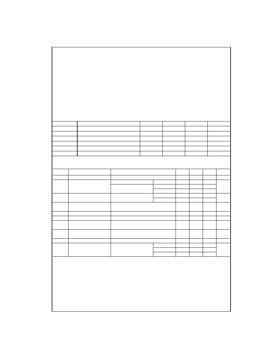
Absolute Maximum Ratings
(Note 1)
Note 1: The "Absolute Maximum Ratings" are those values beyond which
the safety of the device cannot be guaranteed. The device should not be
operated at these limits. The parametric values defined in the Electrical
Characteristics tables are not guaranteed at the absolute maximum ratings.
The "Recommended Operating Conditions" table will define the conditions
for actual device operation.
Recommended Operating Conditions
Electrical Characteristics
over recommended free air temperature range
Supply Voltage
7V
Input Voltage: Control Inputs
7V
Voltage Applied to a Disabled
3-STATE Output
5.5V
Operating Free-Air Temperature Range
0
∞
C to
+
70
∞
C
Storage Temperature Range
-
65
∞
C to
+
150
∞
C
Typical
JA
N Package
58.5
∞
C/W
M Package
77.5
∞
C/W
Symbol
Parameter
Min
Nom
Max
Units
V
CC
Supply Voltage
4.5
5
5.5
V
V
IH
HIGH Level Input Voltage
2
V
V
IL
LOW Level Input Voltage
0.8
V
I
OH
HIGH Level Output Current
-
15
mA
I
OL
LOW Level Output Current
24
mA
T
A
Free Air Operating Temperature
0
70
∞
C
Symbol
Parameter
Test Conditions
Min
Typ
Max
Units
V
IK
Input Clamp Voltage
V
CC
=
Min, I
I
=
-
18 mA
-
1.2
V
V
OH
HIGH Level
V
CC
=
4.5V to 5.5V
I
OH
=
-
0.4 mA
V
CC
-
2
Output Voltage
V
CC
=
Min
I
OH
=
-
3 mA
2.4
3.2
V
I
OH
=
Max
2
V
OL
LOW
Level V
CC
=
Min
I
OL
=
12 mA
0.25
0.4
mA
Output Voltage
I
OL
=
24 mA
0.35
0.5
I
I
Input Current at Maximum
V
CC
=
Max, V
I
=
7V
100
µ
A
Input Voltage
I
IH
HIGH Level Input Current
V
CC
=
Max, V
I
=
2.7V
20
µ
A
I
IL
LOW Level Input Current
V
CC
=
Max, V
I
=
0.4V
-
100
µ
A
I
OZH
HIGH Level 3-STATE
V
CC
=
Max, V
O
=
2.7V
20
µ
A
Output Current
I
OZL
LOW Level 3-STATE
V
CC
=
Max, V
O
=
0.4V
-
20
µ
A
Output Current
I
O
Output Drive Current
V
CC
=
Max, V
O
=
2.25V
-
30
-
112
mA
I
CC
Supply Current
V
CC
=
Max
Outputs HIGH
6
14
Outputs LOW
15
25
mA
Outputs Disabled
13.5
22

www.fairchildsemi.com
4
D
M
74ALS541
Physical Dimensions
inches (millimeters) unless otherwise noted
20-Lead Small Outline Integrated Circuit (SOIC), JEDEC MS-013, 0.300 Wide
Package Number M20B

5
www.fairchildsemi.com
DM74ALS541
Physical Dimensions
inches (millimeters) unless otherwise noted (Continued)
20-Lead Small Outline Package (SOP), EIAJ TYPE II, 5.3mm Wide
Package Number M20D