© 2000 Fairchild Semiconductor Corporation
DS006109
www.fairchildsemi.com
September 1986
Revised February 2000
DM74ALS74A Dual D
Posi
t
i
ve-
Edge-T
r
igg
e
red Fli
p
-F
lop wit
h
Pre
set and C
l
ear
DM74ALS74A
Dual D Positive-Edge-Triggered Flip-Flop
with Preset and Clear
General Description
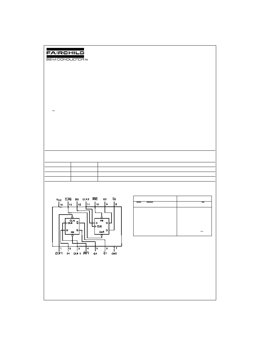
The DM74ALS74A contains two independent positive
edge-triggered flip-flops. Each flip-flop has individual D,
clock, clear and preset inputs, and also complementary Q
and Q outputs.
Information at input D is transferred to the Q output on the
positive going edge of the clock pulse. Clock triggering
occurs at a voltage level of the clock pulse and is not
directly related to the transition time of the positive going
pulse. When the clock input is at either the HIGH or LOW
level, the D input signal has no effect.
Asynchronous preset and clear inputs will set or clear Q
output respectively upon the application of low level signal.
Features
s
Switching specifications at 50 pF
s
Switching specifications guaranteed over full tempera-
ture and V
CC
range
s
Advanced oxide-isolated, ion-implanted Schottky TTL
process
s
Functionally and pin-for-pin compatible with Schottky
and LS TTL counterpart
s
Improved AC performance over LS74 at approximately
half the power
Ordering Code:
Devices also available in Tape and Reel. Specify by appending the suffix letter "X" to the ordering code.
Connection Diagram
Function Table
L
=
LOW State
H
=
HIGH State
X
=
Don't Care
=
Positive Edge Transition
Q
0
=
Previous Condition of Q
Note 1: This condition is nonstable; it will not persist when preset and clear
inputs return to their inactive (HIGH) level. The output levels in this condi-
tion are not guaranteed to meet the V
OH
specification.
Order Number
Package Number Package Description
DM74ALS74AM
M14A
14-Lead Small Outline Integrated Circuit (SOIC), JEDEC MS-012, 0.150 Narrow
DM74ALS74ASJ
M14D
14-Lead Small Outline Package (SOP), EIAJ TYPE II, 5.3mm Wide
DM74ALS74AN
N14A
14-Lead Plastic Dual-In-Line Package (PDIP), JEDEC MS-001, 0.300 Wide
Inputs
Outputs
PR
CLR
CLK
D
Q
Q
L
H
X
X
H
L
H
L
X
X
L
H
L
L
X
X
H (Note 1)
H (Note 1)
H
H
H
H
L
H
H
L
L
H
H
H
L
X
Q
0
Q
0

3
www.fairchildsemi.com
DM74ALS74A
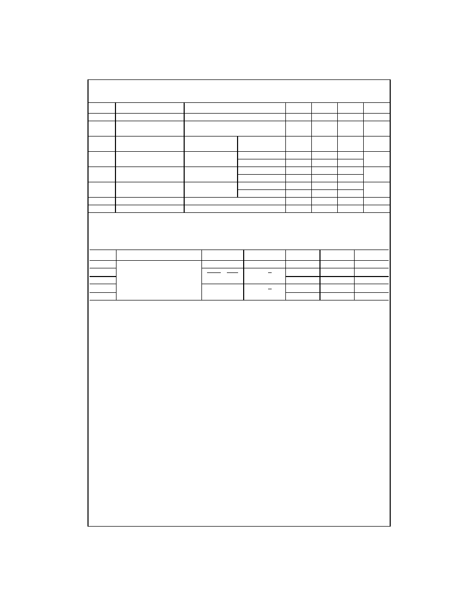
Absolute Maximum Ratings
(Note 2)
Note 2: The "Absolute Maximum Ratings" are those values beyond which
the safety of the device cannot be guaranteed. The device should not be
operated at these limits. The parametric values defined in the Electrical
Characteristics tables are not guaranteed at the absolute maximum ratings.
The "Recommended Operating Conditions" table will define the conditions
for actual device operation.
Recommended Operating Conditions
Note 3: The (
) arrow indicates the positive edge of the Clock is used for reference.
Supply Voltage
7V
Input Voltage
7V
Operating Free Air Temperature Range
0
∞
C to
+
70
∞
C
Storage Temperature Range
-
65
∞
C to
+
150
∞
C
Typical
JA
N Package
87.0
∞
C/W
M Package
117.0
∞
C/W
Symbol
Parameter
Min
Nom
Max
Units
V
CC
Supply Voltage
4.5
5
5.5
V
V
IH
HIGH Level Input Voltage
2
V
V
IL
LOW Level Input Voltage
0.8
V
I
OH
HIGH Level Output Current
-
0.4
mA
I
OL
LOW Level Output Current
8
mA
f
CLK
Clock Frequency
0
34
MHz
t
W(CLK)
Width of Clock Pulse
HIGH
14.5
ns
LOW
14.5
ns
t
W
Pulse Width
LOW
14.5
ns
Preset & Clear
t
SU
Data Setup Time
Data
15
(Note 3)
PRE or CLR
10
(Note 3)
ns
Inactive
t
H
Data Hold Time
0
(Note 3)
ns
T
A
Free Air Operating Temperature
0
70
∞
C
www.fairchildsemi.com
4
D
M
7
4
AL
S7
4
A
Electrical Characteristics
over recommended operating free air temperature range. All typical values are measured at V
CC
=
5V, T
A
=
25
∞
C.
Note 4: I
CC
is measured with D, CLK and PRESET grounded, then with D, CLK and CLEAR grounded.
Note 5: I
IL
PRE and CLR pins not guaranteed to meet specifications with both PRE and CLK LOW.
Switching Characteristics
over recommended operating free air temperature range.
Symbol
Parameter
Conditions
Min
Typ
Max
Units
V
IK
Input Clamp Voltage
V
CC
=
4.5V, I
I
=
-
18 mA
-
1.5
V
V
OH
HIGH Level
I
OH
=
-
0.4 mA
V
CC
-
2
V
Output Voltage
V
CC
=
4.5V to 5.5V
V
OL
LOW Level
V
CC
=
4.5V
I
OL
=
8 mA
0.35
0.5
V
Output Voltage
V
IH
=
2V
I
I
Input Current @
V
CC
=
5.5V,
Clock, D
0.1
mA
Max Input Voltage
V
IH
=
7V
Preset, Clear
0.2
I
IH
HIGH Level
V
CC
=
5.5V,
Clock, D
20
µ
A
Input Current
V
IH
=
2.7V
Preset, Clear
40
I
IL
LOW Level
V
CC
=
5.5V,
Clock, D
-
0.2
mA
Input Current
V
IL
=
0.4V
Preset, Clear (Note 5)
-
0.4
I
O
Output Drive Current
V
CC
=
5.5V, V
O
=
2.25V
-
30
-
112
mA
I
CC
Supply Current
V
CC
=
5.5V (Note 4)
2.4
4
mA
Parameter
Conditions
From
To
Min
Max
Units
f
MAX
V
CC
=
4.5V to 5.5V
34
MHz
t
PLH
R
L
=
500
Preset or Clear
Q or Q
3
13
ns
t
PHL
C
L
=
50 pF
5
15
ns
t
PLH
Clock
Q or Q
5
16
ns
t
PHL
5
18
ns

