© 2000 Fairchild Semiconductor Corporation
DS006244
www.fairchildsemi.com
April 1984
Revised February 2000
DM74ALS874B
Dual
4-
Bit
D-
T
y
p
e
Edge-
T
r
i
ggere
d
Fl
ip-
F
lo
p wit
h
3-ST
A
T
E Outp
uts
DM74ALS874B
Dual 4-Bit D-Type Edge-Triggered Flip-Flop
with 3-STATE Outputs
General Description
This dual 4-bit register features totem-pole 3-STATE out-
puts designed specifically for driving highly-capacitive or
relatively low-impedance loads. The high-impedance state
and increased high-logic-level drive provide this register
with the capability of being connected directly to and driv-
ing the bus lines in a bus-organized system without need
for interface or pull-up components. It is particularly attrac-
tive for implementing buffer registers, I/O ports, bidirec-
tional bus drivers, and working registers.
The eight flip-flops of the DM74ALS874B are edge-trig-
gered D-type flip-flops. On the positive transition of the
clock, the Q outputs will be set to the logic states that were
set up at the D inputs.
A buffered output control input can be used to place the
eight outputs in either a normal logic state (HIGH or LOW
logic levels) or a high-impedance state. In the high-imped-
ance state the outputs neither load nor drive the bus lines
significantly.
The output control does not affect the internal operation of
the flip-flops. That is, the old data can be retained or new
data can be entered even while the outputs are OFF.
Features
s
Switching specifications at 50 pF
s
Switching specifications guaranteed over full tempera-
ture and V
CC
range
s
Advanced oxide-isolated, ion-implanted Schottky TTL
process
s
3-STATE buffer-type outputs drive bus lines directly
s
Space saving 300 mil wide package
s
Asynchronous clear
Ordering Code:
Devices also available in Tape and Reel. Specify by appending the suffix letter "X" to the ordering code.
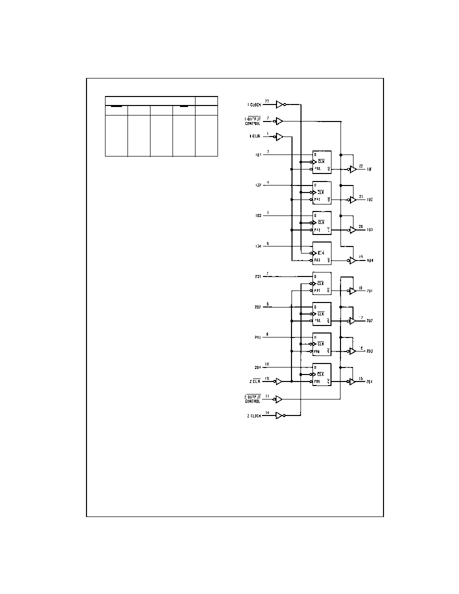
Connection Diagram
Order Number
Package Number
Package Description
DM74ALS874BWM
M24B
24-Lead Small Outline Integrated Circuit (SOIC), JEDEC MS-013, 0.300 Wide
DM74ALS874BNT
N24C
24-Lead Plastic Dual-In-Line Package (PDIP), JEDEC MS-100, 0.300 Wide

3
www.fairchildsemi.com
DM74ALS874B
Absolute Maximum Ratings
(Note 1)
Note 1: The "Absolute Maximum Ratings" are those values beyond which
the safety of the device cannot be guaranteed. The device should not be
operated at these limits. The parametric values defined in the Electrical
Characteristics tables are not guaranteed at the absolute maximum ratings.
The "Recommended Operating Conditions" table will define the conditions
for actual device operation.
Recommended Operating Conditions
Note 2: The (
) arrow indicates the positive edge of the Clock is used for reference.
Supply Voltage
7V
Input Voltage
7V
Voltage Applied to Disabled Output
5.5V
Operating Free Air Temperature Range
0
∞
C to
+
70
∞
C
Storage Temperature Range
-
65
∞
C to
+
150
∞
C
Typical
JA
N Package
51.0
∞
C/W
M Package
86.5
∞
C/W
Symbol
Parameter
Min
Nom
Max
Units
V
CC
Supply Voltage
4.5
5
5.5
V
V
IH
HIGH Level Input Voltage
2
V
V
IL
LOW Level Input Voltage
0.8
V
I
OH
HIGH Level Output Current
-
2.6
mA
I
OL
LOW Level Output Current
24
mA
f
CLK
Clock Frequency
0
30
MHz
t
WCLK
Width of Clock Pulse
HIGH
16.5
ns
LOW
16.5
ns
t
WCLR
Width of Clear Pulse
LOW
10
ns
t
SU
Data Setup Time (Note 2)
15
ns
t
H
Data Hold Time (Note 2)
0
ns
t
SU
Clear Inactive
12
ns
T
A
Free Air Operating Temperature
0
70
∞
C

www.fairchildsemi.com
4
DM
74ALS87
4B
Electrical Characteristics
over recommended operating free air temperature range. All typical values are measured at V
CC
=
5V, T
A
=
25
∞
C.
Switching Characteristics
over recommended operating free air temperature range.
Symbol
Parameter
Conditions
Min
Typ
Max
Units
V
IK
Input Clamp Voltage
V
CC
=
4.5V, I
I
=
-
18 mA
-
1.2
V
V
OH
HIGH Level
V
CC
=
4.5V
I
OH
=
Max
2.4
3.2
V
Output Voltage
V
IL
=
V
IL
Max
V
CC
=
4.5V to 5.5V
I
OH
=
-
400
µ
A
V
CC
-
2
V
V
OL
LOW
Level V
CC
=
4.5V
I
OL
=
12 mA
0.25
0.4
V
Output Voltage
V
IH
=
2V
I
OL
=
24 mA
0.35
0.5
V
I
I
Input Current @Maximum
V
CC
=
5.5V, V
IH
=
7V
0.1
mA
Input Voltage
I
IH
HIGH Level Input Current
V
CC
=
5.5V, V
IH
=
2.7V
20
µ
A
I
IL
LOW Level Input Current
V
CC
=
5.5V, V
IL
=
0.4V
-
0.2
mA
I
O
Output Drive Current
V
CC
=
5.5V, V
O
=
2.25V
-
30
-
112
mA
I
OZH
OFF-State Output Current
V
CC
=
5.5V, V
IH
=
2V
20
µ
A
HIGH Level Voltage Applied
V
O
=
2.7V
I
OZL
OFF-State Output Current
V
CC
=
5.5V, V
IH
=
2V
-
20
µ
A
LOW Level Voltage Applied
V
O
=
0.4V
I
CC
Supply Current
V
CC
=
5.5V
Outputs HIGH
14
21
mA
Outputs OPEN
Outputs LOW
19
30
mA
Outputs Disabled
20
32
mA
Symbol
Parameter
Conditions
From To
Min
Max
Units
f
MAX
Maximum Clock Frequency
V
CC
=
4.5V to 5.5V
30
MHz
t
PLH
Propagation Delay Time
R
L
=
500,
,
Clock
Any Q
4
14
ns
LOW-to-HIGH Level Output
C
L
=
50 pF
t
PHL
Propagation Delay Time
Clock
Any Q
4
14
ns
HIGH-to-LOW Level Output
t
PZH
Output Enable Time
Output
Any Q
4
18
ns
to HIGH Level Output
Control
t
PZL
Output Enable Time
Output
Any Q
4
18
ns
to LOW Level Output
Control
t
PHZ
Output Disable Time
Output
Any Q
2
10
ns
from HIGH Level Output
Control
t
PLZ
Output Disable Time
Output
Any Q
3
12
ns
from LOW Level Output
Control
t
PHL
Propagation Delay Time
Clear
Any Q
5
17
ns
HIGH-to-LOW Level Output

5
www.fairchildsemi.com
DM74ALS874B
Physical Dimensions
inches (millimeters) unless otherwise noted
24-Lead Small Outline Integrated Circuit (SOIC), JEDEC MS-013, 0.300 Wide
Package Number M24B