© 2000 Fairchild Semiconductor Corporation
DS006298
www.fairchildsemi.com
October 1986
Revised March 2000
DM74AS240
∑ DM74AS244
3-ST
A
T
E Bus
Dri
ver/
R
ecei
ver
DM74AS240 ∑ DM74AS244
3-STATE Bus Driver/Receiver
General Description
This family of Advance Schottky 3-STATE Bus circuits are
designed to provide either bidirectional or unidirectional
buffer interface in Memory, Microprocessor, and Communi-
cation Systems. The output characteristics of the circuits
have low impedance sufficient to drive terminated trans-
mission lines down to 133
. The input characteristics of
the circuits likewise have a high impedance so it will not
significantly load the transmission line. The package con-
tains eight 3-STATE buffers organized with four buffers
having a common 3-STATE enable gate. The DM74AS240
and DM74AS244 are eight wide in a 20 pin package, and
may be used as a 4 wide bidirectional or eight wide unidi-
rectional. The buffer selection includes inverting and non-
inverting, with enable or disable 3-STATE control.
Features
s
Advanced oxide-isolated, ion-implanted Schottky TTL
process
s
Improved switching performance with less power dissi-
pation compared with Schottky counterpart
s
Functional and pin compatible with 74LS and Schottky
counterpart
s
Switching response specified into 500
and 50 pF
s
Specified to interface with CMOS at V
OH
=
V
CC
-
2V
Ordering Code:
Devices also available in Tape and Reel. Specify by appending the suffix letter "X" to the ordering code.
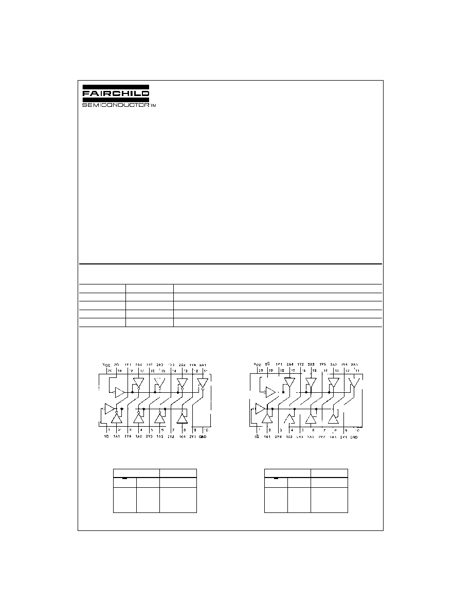
Connection Diagrams
DM74AS240
DM74AS244
Function Tables
DM74AS240
DM74AS244
L
=
LOW Logic Level
H
=
HIGH Logic Level
X
=
Either LOW or HIGH Logic Level
Z
=
High Impedance
Order Number
Package Number
Package Description
DM74AS240WM
M20B
20-Lead Small Outline Integrated Circuit (SOIC), JEDEC MS-013, 0.300 Wide
DM74AS240N
N20A
20-Lead Plastic Dual-In-Line Package (PDIP), JEDEC MS-001, 0.300 Wide
DM74AS244WM
M20B
20-Lead Small Outline Integrated Circuit (SOIC), JEDEC MS-013, 0.300 Wide
DM74AS244N
N20A
20-Lead Plastic Dual-In-Line Package (PDIP), JEDEC MS-001, 0.300 Wide
Inputs
Output
G
A
Y
L
L
H
L
H
L
H
X
Z
Inputs
Output
G
A
Y
L
L
L
L
H
H
H
X
Z
www.fairchildsemi.com
2
DM
74AS240
∑ DM
74AS244
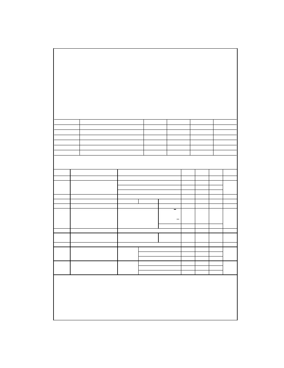
Absolute Maximum Ratings
(Note 1)
Note 1: The "Absolute Maximum Ratings" are those values beyond which
the safety of the device cannot be guaranteed. The device should not be
operated at these limits. The parametric values defined in the Electrical
Characteristics tables are not guaranteed at the absolute maximum ratings.
The "Recommended Operating Conditions" table will define the conditions
for actual device operation.
Recommended Operating Conditions
Electrical Characteristics
over recommended operating free air temperature range. All typical values are measured at V
CC
=
5V, T
A
=
25
∞
C.
Note 2: The output conditions have been chosen to produce a current that closely approximates one half the true short-circuit output current, I
OS
.
Supply Voltage, V
CC
7V
Input Voltage
7V
Voltage Applied to Disabled Output
5.5V
Operating Free Air Temperature Range
0
∞
C to
+
70
∞
C
Storage Temperature Range
-
65
∞
C to
+
150
∞
C
Typical
JA
N Package
57.0
∞
C/W
M Package
76.0
∞
C/W
Symbol
Parameter
Min
Nom
Max
Units
V
CC
Supply Voltage
4.5
5
5.5
V
V
IH
HIGH Level Input Voltage
2
V
V
IL
LOW Level Input Voltage
0.8
V
I
OH
HIGH Level Output Current
-
15
mA
I
OL
LOW Level Output Current
64
mA
T
A
Free Air Operating Temperature
0
70
∞
C
Symbol
Parameter
Conditions
Min
Typ
Max
Units
V
IK
Input Clamp Voltage
V
CC
=
4.5V, I
IN
=
-
18 mA
-
1.2
V
V
OH
HIGH Level
V
CC
=
4.5V, I
OH
=
-
3 mA
2.4
3.2
V
Output Voltage
V
CC
=
4.5V, I
OH
=
Max
2.4
I
OH
=
-
2 mA, V
CC
=
4.5V to 5.5V
V
CC
-
2
V
OL
LOW Level Output Voltage
V
CC
=
4.5V, I
OL
=
Max
0.35
0.55
V
I
I
Input Current at Max Input Voltage
V
CC
=
5.5V
V
IN
=
7V
Others
100
µ
A
I
IH
HIGH Level Input Current
V
CC
=
5.5V, V
IN
=
2.7V
Others
20
µ
A
I
IL
LOW Level Input Current
V
CC
=
5.5V, V
IN
=
0.4V
AS240, (G, G),
µ
A
(Control Inputs),
-
500
DM74AS244 (G)
DM74AS244 (A)
-
1000
I
OZH
HIGH Level 3-STATE Output Current V
CC
=
5.5V, V
=
2.7V
50
µ
A
I
OZL
LOW Level 3-STATE
V
CC
=
5.5V, V
=
0.4V
DM74AS240,
-
50
µ
A
Output Current
DM74AS244
I
O
(Note 2)
Output Drive Current
V
CC
=
5.5V, V
OUT
=
2.25V
-
50
-
115
-
150
mA
I
CC
DM74AS240
V
CC
=
5.5V
Outputs HIGH
11
17
Supply Current
Outputs LOW
51
75
mA
3-STATE
24
38
I
CC
DM74AS244
V
CC
=
5.5V
Outputs HIGH
22
34
Supply Current
Outputs LOW
60
90
mA
3-STATE
34
54
3
www.fairchildsemi.com
DM74AS240
∑ DM74AS244
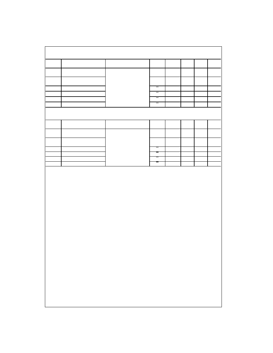
DM74AS240 Switching Characteristics
over recommended operating free air temperature range
DM74AS244 Switching Characteristics
over recommended operating free air temperature range
Symbol
Parameter
Conditions
From
To
Min
Max
Units
(Input)
(Output)
t
PLH
Propagation Delay Time
V
CC
=
4.5V to 5.5V
A
Y
2
6.5
ns
LOW-to-HIGH Level Output
R
1
=
R
2
=
500
t
PHL
Propagation Delay Time
C
L
=
50 pF
A
Y
2
5.7
ns
HIGH-to-LOW Level Output
t
PZL
Output Enable to LOW Level
G
Y
2
9
ns
t
PZH
Output Enable to HIGH Level
G
Y
2
6.4
ns
t
PLZ
Output Disable from LOW Level
G
Y
2
9.5
ns
t
PHZ
Output Disable from HIGH Level
G
Y
2
5
ns
Symbol
Parameter
Conditions
From
To
Min
Max
Units
(Input)
(Output)
t
PLH
Propagation Delay Time
V
CC
=
4.5V to 5.5V
A
Y
2
6.2
ns
LOW-to-HIGH Level Output
R
1
=
R
2
=
500
t
PHL
Propagation Delay Time
C
L
=
50 pF
A
Y
2
6.2
ns
HIGH-to-LOW Level Output
t
PZL
Output Enable to LOW Level
G
Y
2
7.5
ns
t
PZH
Output Enable to HIGH Level
G
Y
2
9
ns
t
PLZ
Output Disable from LOW Level
G
Y
2
9
ns
t
PHZ
Output Disable from HIGH Level
G
Y
2
6
ns

www.fairchildsemi.com
4
DM
74AS240
∑ DM
74AS244
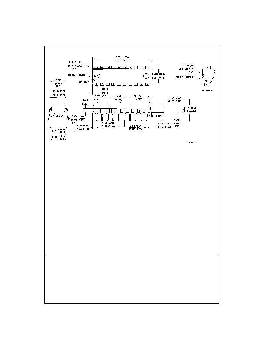
Physical Dimensions
inches (millimeters) unless otherwise noted
20-Lead Small Outline Integrated Circuit (SOIC), JEDEC MS-013, 0.300 Wide
Package Number M20B
5
www.fairchildsemi.com
DM74AS240
∑ DM74AS244
3-ST
A
T
E Bus
Dri
ver/
R
ecei
ver
Physical Dimensions
inches (millimeters) unless otherwise noted (Continued)
20-Lead Plastic Dual-In-Line Package (PDIP), JEDEC MS-001, 0.300 Wide
Package Number N20A
Fairchild does not assume any responsibility for use of any circuitry described, no circuit patent licenses are implied and
Fairchild reserves the right at any time without notice to change said circuitry and specifications.
LIFE SUPPORT POLICY
FAIRCHILD'S PRODUCTS ARE NOT AUTHORIZED FOR USE AS CRITICAL COMPONENTS IN LIFE SUPPORT
DEVICES OR SYSTEMS WITHOUT THE EXPRESS WRITTEN APPROVAL OF THE PRESIDENT OF FAIRCHILD
SEMICONDUCTOR CORPORATION. As used herein:
1. Life support devices or systems are devices or systems
which, (a) are intended for surgical implant into the
body, or (b) support or sustain life, and (c) whose failure
to perform when properly used in accordance with
instructions for use provided in the labeling, can be rea-
sonably expected to result in a significant injury to the
user.
2. A critical component in any component of a life support
device or system whose failure to perform can be rea-
sonably expected to cause the failure of the life support
device or system, or to affect its safety or effectiveness.
www.fairchildsemi.com