© 2000 Fairchild Semiconductor Corporation
DS006314
www.fairchildsemi.com
October 1986
Revised March 2000
DM74AS574 Octal
D-
T
ype E
d
ge-T
r
igger
ed
F
l
i
p
-Fl
ops w
i
th 3-
ST
A
T
E O
u
t
put
s
DM74AS574
Octal D-Type Edge-Triggered Flip-Flops
with 3-STATE Outputs
General Description
These 8-bit registers feature totem-pole 3-STATE outputs
designed specifically for driving highly-capacitive or rela-
tively low-impedance loads. The high-impedance state and
increased HIGH-logic-level drive provide these registers
with the capability of being connected directly to and driv-
ing the bus lines in a bus-organized system without need
for interface or pull-up components. They are particularly
attractive for implementing buffer registers, I/O ports, bidi-
rectional bus drivers, and working registers.
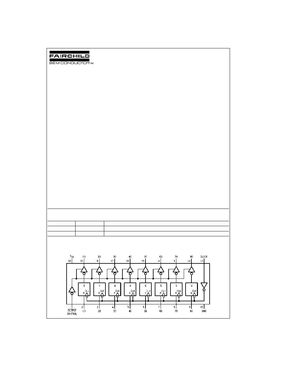
The eight flip-flops of the DM74AS574 are edge-triggered
D-type flip-flops. On the positive transition of the clock, the
Q outputs will be set to the logic states that were set up at
the D inputs.
A buffered output control input can be used to place the
eight outputs in either a normal logic state (HIGH or LOW
logic levels) or a high impedance state. In the high-imped-
ance state the outputs neither load nor drive the bus lines
significantly.
The output control does not affect the internal operation of
the flip-flops. That is, the old data can be retained or new
data can be entered even while the outputs are OFF.
The pinout is arranged to ease printed circuit board layout.
All data inputs are on one side of the package while all the
outputs are on the other side.
Features
s
Switching specifications at 50 pF
s
Switching specifications guaranteed over full tempera-
ture and V
CC
range
s
Advanced oxide-isolated, ion-implanted Schottky TTL
process
s
Functionally equivalent with DM74S374
s
Improved AC performance over DM74S374 at approxi-
mately half the power
s
3-STATE buffer-type outputs drive bus lines directly
s
Bus structured pinout
Ordering Code:
Devices also available in Tape and Reel. Specify by appending the suffix letter "X" to the ordering code.
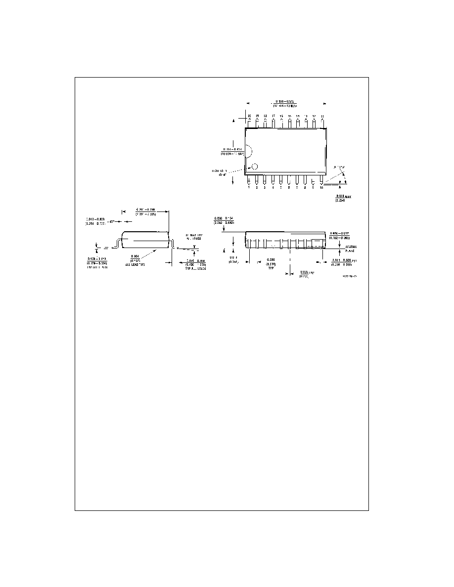
Connection Diagram
Order Number
Package Number
Package Description
DM74AS574WM
M20B
20-Lead Small Outline Integrated Circuit (SOIC), JEDEC MS-013, 0.300 Wide
DM74AS574N
N20A
20-Lead Plastic Dual-In-Line Package (PDIP), JEDEC MS-001, 0.300 Wide

3
www.fairchildsemi.com
DM74AS574
Absolute Maximum Ratings
(Note 1)
Note 1: The "Absolute Maximum Ratings" are those values beyond which
the safety of the device cannot be guaranteed. The device should not be
operated at these limits. The parametric values defined in the Electrical
Characteristics tables are not guaranteed at the absolute maximum ratings.
The "Recommended Operating Conditions" table will define the conditions
for actual device operation.
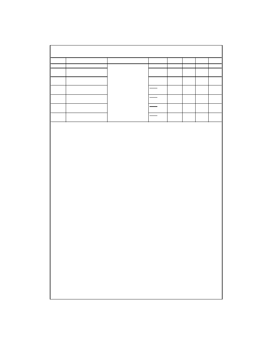
Recommended Operating Conditions
Note 2: The (
) arrow indicates the positive edge of the clock is used for reference.
Electrical Characteristics
over recommended operating free air temperature range. All typical values are measured at V
CC
=
5V, T
A
=
25
∞
C.
Note 3: The output conditions have been chosen to produce a current that closely approximates one half of the true short circuit output current, I
OS
.
Supply Voltage
7V
Input Voltage
7V
Voltage Applied to Disabled Output
5.5V
Operating Free Air Temperature Range
0
∞
C to
+
70
∞
C
Storage Temperature Range
-
65
∞
C to
+
150
∞
C
Typical
JA
N Package
52.0
∞
C/W
M Package
70.0
∞
C/W
Symbol
Parameter
Min
Nom
Max
Units
V
CC
Supply Voltage
4.5
5
5.5
V
V
IH
HIGH Level Input Voltage
2
V
V
IL
LOW Level Input Voltage
0.8
V
I
OH
HIGH Level Output Current
-
15
mA
I
OL
LOW Level Output Current
48
mA
f
CLK
Clock Frequency
0
80
MHz
t
WCLK
Width of Clock Pulse
HIGH
4
ns
LOW
6
t
SU
Data Setup Time (Note 2)
4
ns
t
H
Data Hold Time (Note 2)
2
ns
T
A
Free Air Operating Temperature
0
70
∞
C
Symbol
Parameter
Conditions
Min
Typ
Max
Units
V
IK
Input Clamp Voltage
V
CC
=
4.5V, I
I
=
-
18 mA
-
1.2
V
V
OH
HIGH Level
V
CC
=
4.5V, V
IL
=
V
IL
Max,
2.4
3.2
Output Voltage
I
OH
=
Max
V
I
OH
=
-
2 mA, V
CC
=
4.5V to 5.5V
V
CC
-
2
V
OL
LOW
Level V
CC
=
4.5V, V
IH
=
2V,
0.35
0.5
V
Output Voltage
I
OL
=
Max
I
I
Input Current @ Max Input Voltage V
CC
=
5.5V, V
IH
=
7V
0.1
mA
I
IH
HIGH Level Input Current
V
CC
=
5.5V, V
IH
=
2.7V
20
µ
A
I
IL
LOW Level Input Current
V
CC
=
5.5V, V
IL
=
0.4V
-
0.5
mA
I
O
(Note 3)
Output Drive Current
V
CC
=
5.5V, V
O
=
2.25V
-
30
-
112
mA
I
OZH
OFF-State Output Current,
V
CC
=
5.5V, V
IH
=
2V,
50
µ
A
HIGH Level Voltage Applied
V
O
=
2.7V
I
OZL
OFF-State Output Current,
V
CC
=
5.5V, V
IH
=
2V,
-
50
µ
A
LOW Level Voltage Applied
V
O
=
0.4V
I
CC
Supply Current
V
CC
=
5.5V
Outputs HIGH
73
116
Outputs Open
Outputs LOW
85
134
mA
Outputs Disabled
84
134