 | –≠–ª–µ–∫—Ç—Ä–æ–Ω–Ω—ã–π –∫–æ–º–ø–æ–Ω–µ–Ω—Ç: DM74AS640 | –°–∫–∞—á–∞—Ç—å:  PDF PDF  ZIP ZIP |

© 2000 Fairchild Semiconductor Corporation
DS006708
www.fairchildsemi.com
October 1986
Revised March 2000
DM74AS640
3-
S
T
A
T
E Oct
a
l
Bus
T
r
ansce
iver
DM74AS640
3-STATE Octal Bus Transceiver
General Description
This advanced Schottky device contains 8 pairs of 3-
STATE logic elements configured as octal bus transceiver.
This circuit is designed for use in memory, microprocessor
systems and in asynchronous bidirectional data buses.
This device transmits data from the A bus to the B bus, or
vice versa, depending upon the logic level of the direction
control input (DIR). The enable input (G) can be used to
disable the devices, effecting isolation of buses A and B.
The 3-STATE circuitry also contains a protection feature
that prevents these transceivers from glitching the bus dur-
ing power-up or power-down.
Features
s
Switching specifications at 50 pF
s
Switching specifications guaranteed over full tempera-
ture and V
CC
range
s
Advanced oxide-isolated, ion-implanted Schottky TTL
process
s
Functionally and pin for pin compatible with Schottky,
low power Schottky, and advanced low power Schottky
TTL counterpart
s
Improved AC performance over Schottky, low power
Schottky, and advanced low power Schottky counter-
parts
s
3-STATE outputs independently controlled on A and B
buses
s
Low output impedance drive to drive terminated trans-
mission lines to 133
s
Specified to interface with CMOS at V
OH
=
V
CC
-
2V
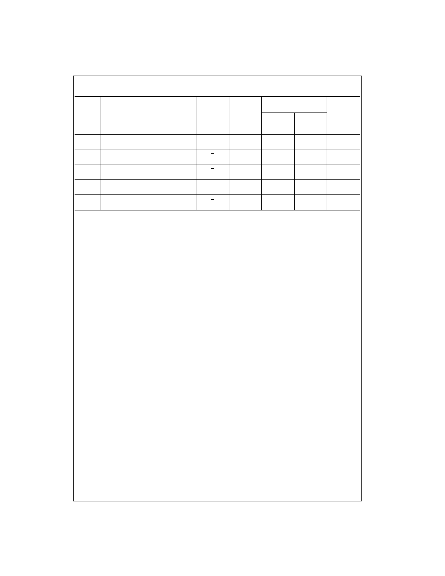
Ordering Code:
Devices also available in Tape and Reel. Specify by appending the suffix letter "X" to the ordering code.
Connection Diagram
Top View
Function Table
H
=
HIGH Logic Level
L
=
LOW Logic Level
X
=
Immaterial
Logic Diagram
Order Number
Package Number
Package Description
DM74AS640WM
M20B
20-Lead Small Outline Integrated Circuit (SOIC), JEDEC MS-013, 0.300 Wide
DM74AS640N
N20A
20-Lead Plastic Dual-In-Line Package (PDIP), JEDEC MS-001, 0.300 Wide
Control Inputs
Operation
G
DIR
L
L
B Data to A Bus
L
H
A Data to B Bus
H
X
Isolation

www.fairchildsemi.com
2
DM
74AS640
Absolute Maximum Ratings
(Note 1)
Note 1: The "Absolute Maximum Ratings" are those values beyond which
the safety of the device cannot be guaranteed. The device should not be
operated at these limits. The parametric values defined in the Electrical
Characteristics tables are not guaranteed at the absolute maximum ratings.
The "Recommended Operating Conditions" table will define the conditions
for actual device operation.
Recommended Operating Conditions
Electrical Characteristics
over recommended operating free air temperature range (unless otherwise noted)
Note 2: All typicals are at V
CC
=
5.0V, T
A
=
25
∞
C.
Note 3: For I/O ports, the parameters I
IH
and I
IL
include the OFF-State output current, I
OZH
and I
OZL
.
Supply Voltage
7V
Input Voltage
Control Inputs
7V
I/O Ports
5.5V
Operating Free Air Temperature Range
0
∞
C to
+
70
∞
C
Storage Temperature Range
-
65
∞
C to
+
150
∞
C
Typical
JA
N Package
51.5
∞
C
M Package
69.0
∞
C
Symbol
Parameter
Min
Typ
Max
Units
V
CC
Supply Voltage
4.5
5
5.5
V
V
IH
HIGH Level Input Voltage
2
V
V
IL
LOW Level Input Voltage
0.8
V
I
OH
HIGH Level Output Current
-
15
mA
I
OL
LOW Level Output Current
64
mA
T
A
Free Air Operating Temperature
0
70
∞
C
Symbol
Parameter
Conditions
Min
Typ
Max
Units
(Note 2)
V
I
Input Clamp Voltage
V
CC
=
Min, I
I
=
-
18 mA
-
1.2
V
V
OH
HIGH Level
V
CC
=
4.5V to 5.5V, I
OH
=
-
2 mA
V
CC
-
2
V
Output Voltage
V
CC
=
4.5V, I
OH
=
-
3 mA
2.4
V
V
CC
=
4.5V, I
OH
=
Max
2.4
V
V
OL
LOW Level Output Voltage
V
CC
=
Min, I
OL
=
Max
0.35
0.55
V
I
I
Input Current at Max
V
CC
=
Max, V
I
=
7V,
0.1
mA
Input Voltage
(V
I
=
5.5V for A or B Ports)
I
IH
HIGH Level
V
CC
=
Max
Control Inputs
20
µ
A
Input Current
V
I
=
2.7V (Note 3)
A or B Ports
70
I
IL
LOW Level
V
CC
=
Max,
Control Inputs
-
0.5
mA
Input Current
V
I
=
0.4V (Note 3)
A or B Ports
-
0.75
I
O
Output Drive Current
V
CC
=
Max, V
O
=
2.25V
-
50
-
150
mA
I
CCH
Supply Current with Outputs HIGH
V
CC
=
Max
37
58
mA
I
CCL
Supply Current with Outputs LOW
78
123
mA
I
CCZ
Supply Current with Outputs
51
80
mA
in 3-STATE
3
www.fairchildsemi.com
DM74AS640
Switching Characteristics
over recommended operating free air temperature range (unless otherwise noted)
From
To
V
CC
=
Min to Max,
Symbol
Parameter
(Input)
(Output)
C
L
=
50 pF, R
1
=
R
2
=
500
Units
Min
Max
t
PLH
Propagation Delay Time
A or B
B or A
2
7
ns
LOW-to-HIGH Level Output
t
PHL
Propagation Delay Time
A or B
B or A
2
6
ns
HIGH-to-LOW Level Output
t
PZH
Output Enable Time to
G
A or B
2
8
ns
HIGH Level Output
t
PZL
Output Enable Time to
G
A or B
2
10
ns
LOW Level Output
t
PHZ
Output Disable Time from
G
A or B
2
8
ns
HIGH Level Output
t
PLZ
Output Disable Time from
G
A or B
2
13
ns
LOW Level Output
www.fairchildsemi.com
4
DM
74AS640
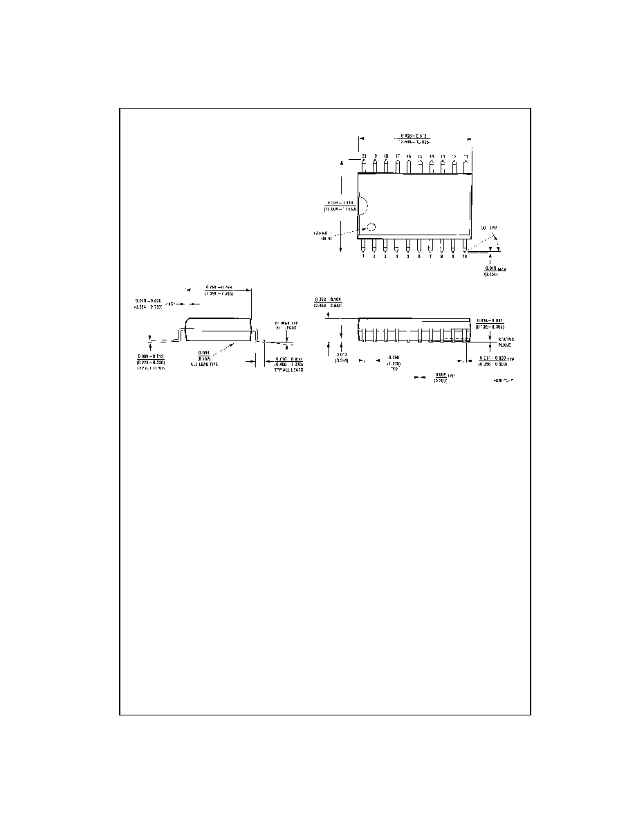
Physical Dimensions
inches (millimeters) unless otherwise noted
20-Lead Small Outline Integrated Circuit (SOIC), JEDEC MS-013, 0.300 Wide
Package Number M20B
5
www.fairchildsemi.com
DM74AS640
3-
S
T
A
T
E Oct
a
l
Bus
T
r
ansce
iver
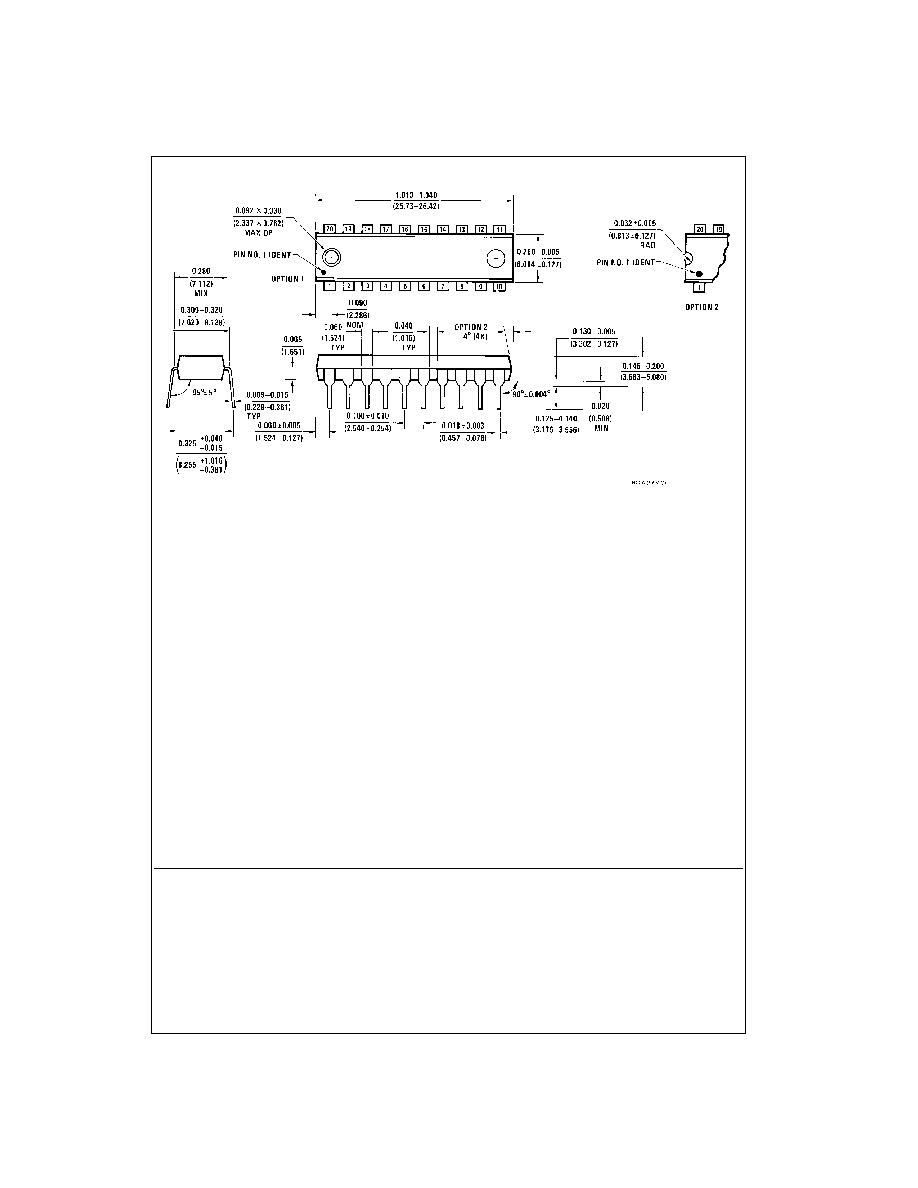
Physical Dimensions
inches (millimeters) unless otherwise noted (Continued)
20-Lead Plastic Dual-In-Line Package (PDIP), JEDEC MS-001, 0.300 Wide
Package Number N20A
Fairchild does not assume any responsibility for use of any circuitry described, no circuit patent licenses are implied and
Fairchild reserves the right at any time without notice to change said circuitry and specifications.
LIFE SUPPORT POLICY
FAIRCHILD'S PRODUCTS ARE NOT AUTHORIZED FOR USE AS CRITICAL COMPONENTS IN LIFE SUPPORT
DEVICES OR SYSTEMS WITHOUT THE EXPRESS WRITTEN APPROVAL OF THE PRESIDENT OF FAIRCHILD
SEMICONDUCTOR CORPORATION. As used herein:
1. Life support devices or systems are devices or systems
which, (a) are intended for surgical implant into the
body, or (b) support or sustain life, and (c) whose failure
to perform when properly used in accordance with
instructions for use provided in the labeling, can be rea-
sonably expected to result in a significant injury to the
user.
2. A critical component in any component of a life support
device or system whose failure to perform can be rea-
sonably expected to cause the failure of the life support
device or system, or to affect its safety or effectiveness.
www.fairchildsemi.com