© 2000 Fairchild Semiconductor Corporation
DS006392
www.fairchildsemi.com
August 1986
Revised March 2000
DM74LS151
1-
of-
8
Li
ne
Data
Sele
ctor
/Mult
i
p
lexer
DM74LS151
1-of-8 Line Data Selector/Multiplexer
General Description
This data selector/multiplexer contains full on-chip decod-
ing to select the desired data source. The DM74LS151
selects one-of-eight data sources. The DM74LS151 has a
strobe input which must be at a low logic level to enable
these devices. A high level at the strobe forces the W out-
put HIGH, and the Y output LOW.
The DM74LS151 features complementary W and Y out-
puts.
Features
s
Select one-of-eight data lines
s
Performs parallel-to-serial conversion
s
Permits multiplexing from N lines to one line
s
Also for use as Boolean function generator
s
Typical average propagation delay time data input to
W output 12.5 ns
s
Typical power dissipation 30 mW
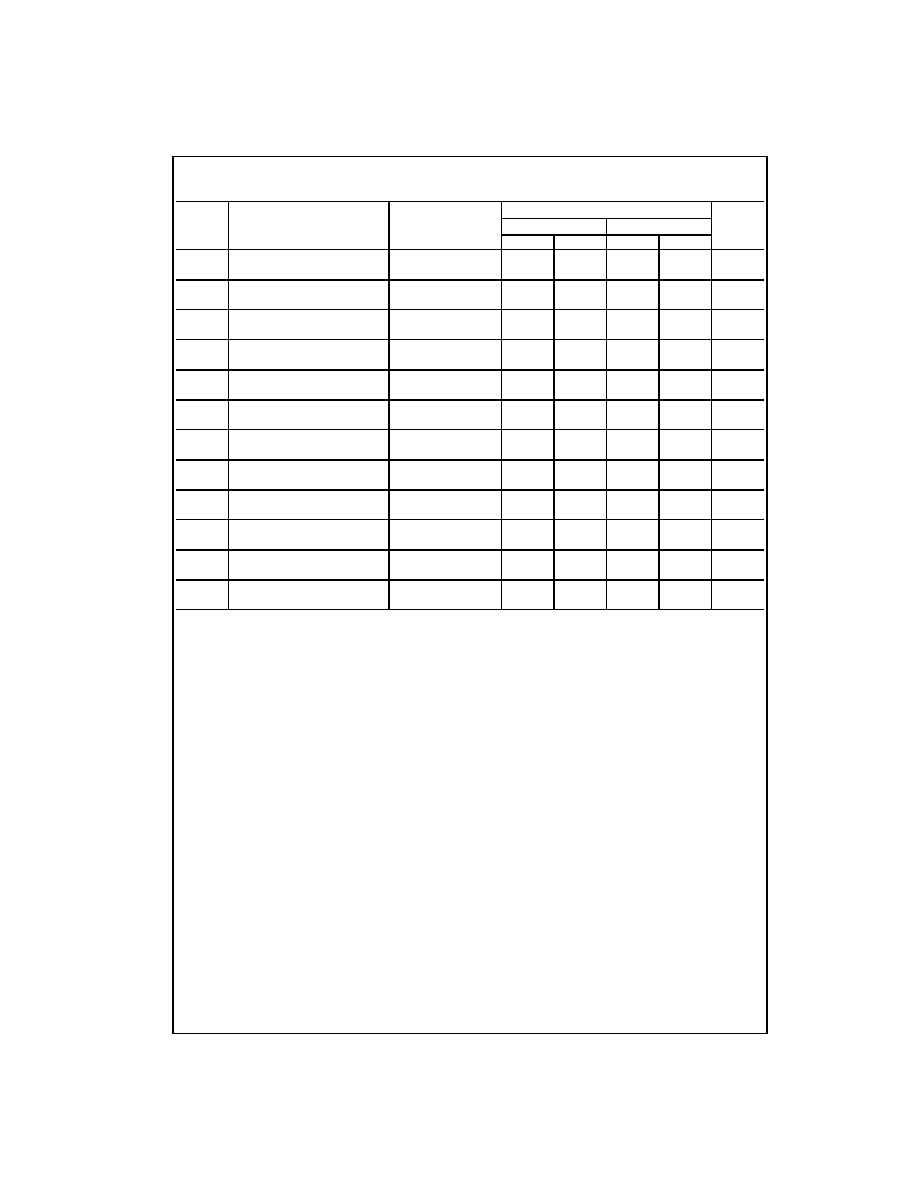
Ordering Code:
Devices also available in Tape and Reel. Specify by appending the suffix letter "X" to the ordering code.
Connection Diagram
Truth Table
H
=
HIGH Level
L
=
LOW Level
X
=
Don't Care
D0, D1...D7
=
the level of the respective D input
Order Number
Package Number
Package Description
DM74LS151M
M16A
16-Lead Small Outline Integrated Circuit (SOIC), JEDEC MS-012, 0.150 Narrow
DM74LS151SJ
M16D
16-Lead Small Outline Package (SOP), EIAJ TYPE II, 5.3mm Wide
DM74LS151N
N16E
16-Lead Plastic Dual-In-Line Package (PDIP), JEDEC MS-001, 0.300 Wide
Inputs
Outputs
Select
Strobe
Y
W
C
B
A
S
X
X
X
H
L
H
L
L
L
L
D0
D0
L
L
H
L
D1
D1
L
H
L
L
D2
D2
L
H
H
L
D3
D3
H
L
L
L
D4
D4
H
L
H
L
D5
D5
H
H
L
L
D6
D6
H
H
H
L
D7
D7
3
www.fairchildsemi.com
DM74LS151
Absolute Maximum Ratings
(Note 1)
Note 1: The "Absolute Maximum Ratings" are those values beyond which
the safety of the device cannot be guaranteed. The device should not be
operated at these limits. The parametric values defined in the Electrical
Characteristics tables are not guaranteed at the absolute maximum ratings.
The "Recommended Operating Conditions" table will define the conditions
for actual device operation.
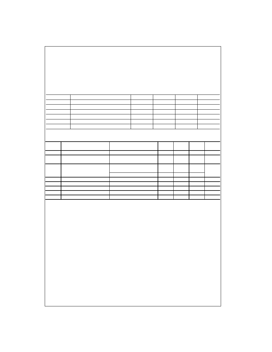
Recommended Operating Conditions
Electrical Characteristics
over recommended operating free air temperature range (unless otherwise noted)
Note 2: All typicals are at V
CC
=
5V, T
A
=
25
∞
C.
Note 3: Not more than one output should be shorted at a time, and the duration should not exceed one second.
Note 4: I
CC
is measured with all outputs OPEN, strobe and data select inputs at 4.5V, and all other inputs OPEN.
Supply Voltage
7V
Input Voltage
7V
Operating Free Air Temperature Range
0
∞
C to
+
70
∞
C
Storage Temperature Range
-
65
∞
C to
+
150
∞
C
Symbol
Parameter
Min
Nom
Max
Units
V
CC
Supply Voltage
4.75
5
5.25
V
V
IH
HIGH Level Input Voltage
2
V
V
IL
LOW Level Input Voltage
0.8
V
I
OH
HIGH Level Output Current
-
0.4
mA
I
OL
LOW Level Output Current
8
mA
T
A
Free Air Operating Temperature
0
70
∞
C
Symbol
Parameter
Conditions
Min
Typ
Max
Units
(Note 2)
V
I
Input Clamp Voltage
V
CC
=
Min, I
I
=
-
18 mA
-
1.5
V
V
OH
HIGH Level
V
CC
=
Min, I
OH
=
Max
2.7
3.4
V
Output Voltage
V
IL
=
Max, V
IH
=
Min
V
OL
LOW
Level V
CC
=
Min, I
OL
=
Max
0.35
0.5
Output Voltage
V
IL
=
Max, V
IH
=
Min
V
I
OL
=
4 mA, V
CC
=
Min
0.25
0.4
I
I
Input Current @ Max Input Voltage
V
CC
=
Max, V
I
=
7V
0.1
mA
I
IH
HIGH Level Input Current
V
CC
=
Max, V
I
=
2.7V
20
µ
A
I
IL
LOW Level Input Current
V
CC
=
Max, V
I
=
0.4V
-
0.4
mA
I
OS
Short Circuit Output Current
V
CC
=
Max (Note 3)
-
20
-
100
mA
I
CC
Supply Current
V
CC
=
Max (Note 4)
6
10
mA

5
www.fairchildsemi.com
DM74LS151
Physical Dimensions
inches (millimeters) unless otherwise noted
16-Lead Small Outline Integrated Circuit (SOIC), JEDEC MS-012, 0.150 Narrow
Package Number M16A