DM74LS169A
Synchronous 4-Bit Up/Down Binary Counter
General Description
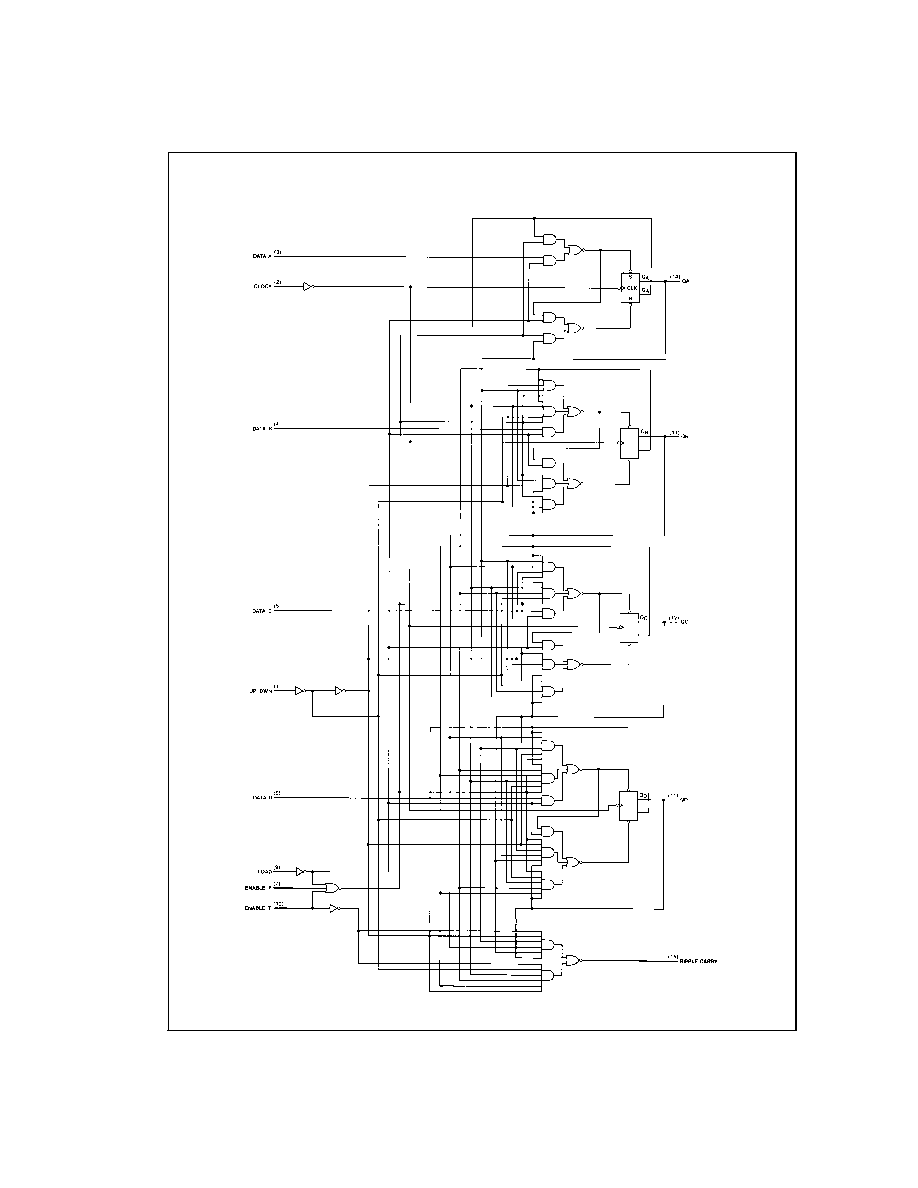
This synchronous presettable counter features an internal
carry look-ahead for cascading in high-speed counting appli-
cations. Synchronous operation is provided by having all
flip-flops clocked simultaneously, so that the outputs all
change at the same time when so instructed by the
count-enable inputs and internal gating. This mode of opera-
tion helps eliminate the output counting spikes that are nor-
mally associated with asynchronous (ripple clock) counters.
A buffered clock input triggers the four master-slave flip-flops
on the rising edge of the clock waveform.
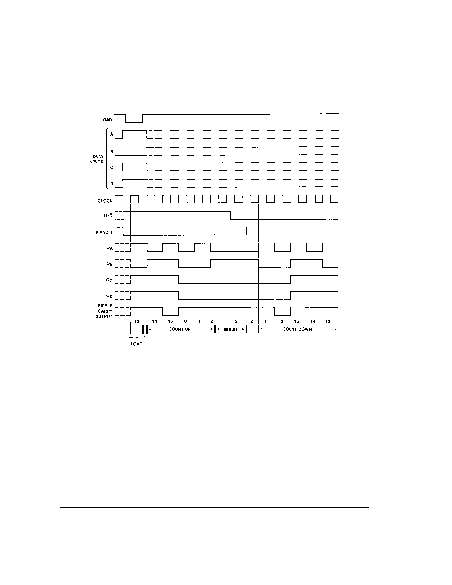
This counter is fully programmable; that is, the outputs may
each be preset either high or low. The load input circuitry al-
lows loading with the carry-enable output of cascaded
counters. As loading is synchronous, setting up a low level at
the load input disables the counter and causes the outputs to
agree with the data inputs after the next clock pulse.
The carry look-ahead circuitry permits cascading counters
for n-bit synchronous applications without additional gating.
Both count-enable inputs (P and T) must be low to count.
The direction of the count is determined by the level of the
up/down input. When the input is high, the counter counts
up; when low, it counts down. Input T is fed forward to enable
the carry outputs. The carry output thus enabled will produce
a low-level output pulse with a duration approximately equal
to the high portion of the Q
A
output when counting up, and
approximately equal to the low portion of the Q
A
output when
counting down. This low-level overflow carry pulse can be
used to enable successively cascaded stages. Transitions at
the enable P or T inputs are allowed regardless of the level
of the clock input. All inputs are diode clamped to minimize
transmission-line effects, thereby simplifying system design.
This counter features a fully independent clock circuit.
Changes at control inputs (enable P, enable T, load, up/
down), which modify the operating mode, have no effect until
clocking occurs. The function of the counter (whether en-
abled, disabled, loading, or counting) will be dictated solely
by the conditions meeting the stable setup and hold times.
Features
n
Fully synchronous operation for counting and
programming.
n
Internal look-ahead for fast counting.
n
Carry output for n-bit cascading.
n
Fully independent clock circuit
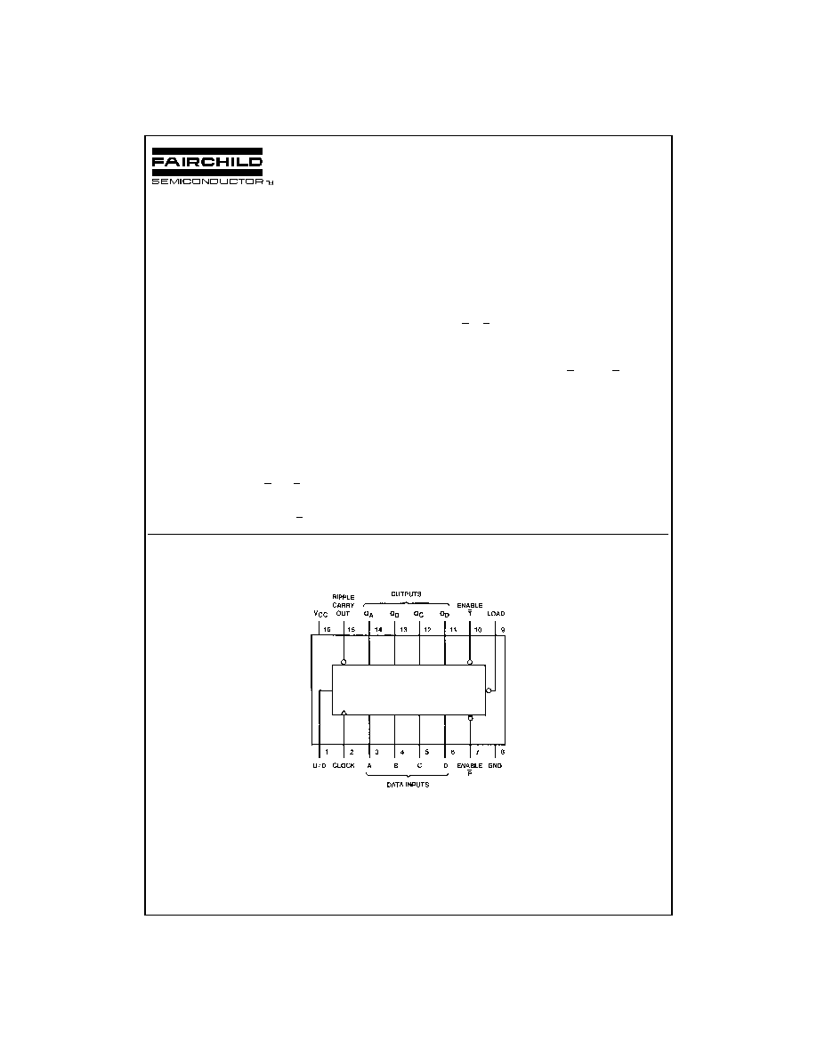
Connection Diagram
Dual-In-Line Package
DS006401-1
Order Number 54LS169DMQB, 54LS169FMQB, 54LS169LMQB,
DM54LS169AJ, DM54LS169AW, DM74LS169AM or DM74LS169AN
See Package Number E20A, J16A, M16A, N16E or W16A
April 1998
DM74LS169A
Synchronous
4-Bit
Up/Down
Binary
Counter
© 1998 Fairchild Semiconductor Corporation
DS006401
www.fairchildsemi.com
Absolute Maximum Ratings
(Note 1)
Supply Voltage
7V
Input Voltage
7V
Operating Free Air Temperature Range
DM54LS and 54LS
-55°C to +125°C
DM74LS
0°C to +70°C
Storage Temperature Range
-65°C to +150°C
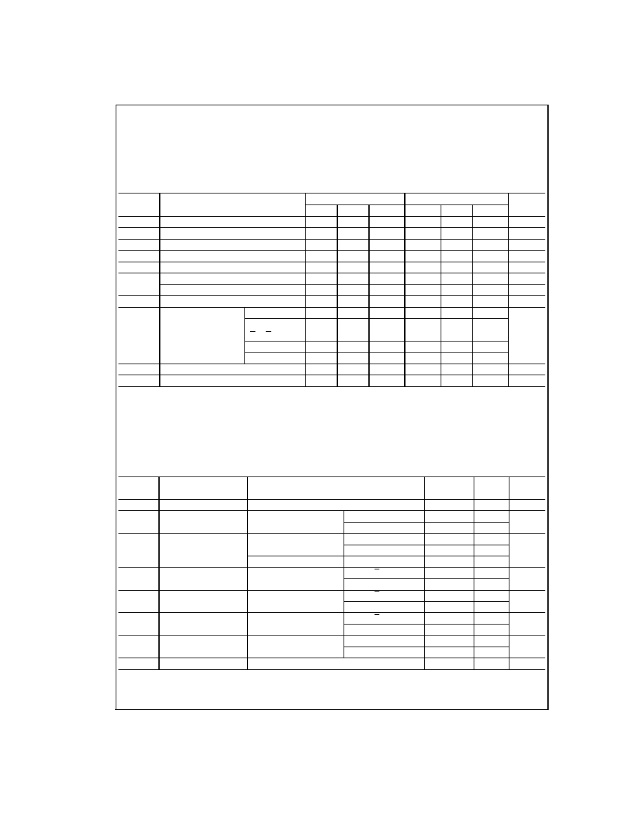
Recommended Operating Conditions
Symbol
Parameter
DM54LS169A
DM74LS169A
Units
Min
Nom
Max
Min
Nom
Max
V
CC
Supply Voltage
4.5
5
5.5
4.75
5
5.25
V
V
IH
High Level Input Voltage
2
2
V
V
IL
Low Level Input Voltage
0.7
0.8
V
I
OH
High Level Output Current
-0.4
-0.4
mA
I
OL
Low Level Output Current
4
8
mA
f
CLK
Clock Frequency (Note 2)
0
25
0
25
MHz
Clock Frequency (Note 3)
0
20
0
20
MHz
t
W
Clock Pulse Width (Note 4)
25
25
ns
t
SU
Setup Time
Data
20
20
(Note 4)
Enable
20
20
T or P
ns
Load
25
25
U/D
30
30
t
H
Hold Time (Note 4)
0
0
ns
T
A
Free Air Operating Temperature
-55
125
0
70
°C
Note 1:
The "Absolute Maximum Ratings" are those values beyond which the safety of the device cannot be guaranteed. The device should not be operated at these
limits. The parametric values defined in the "Electrical Characteristics" table are not guaranteed at the absolute maximum ratings. The "Recommended Operating
Conditions" table will define the conditions for actual device operation.
Note 2: C
L
= 15 pF, R
L
= 2 k
, T
A
= 25°C and V
CC
= 5V.
Note 3: C
L
= 50 pF, R
L
= 2 k
, T
A
= 25°C and V
CC
= 5V.
Note 4: T
A
= 25°C and V
CC
= 5V.
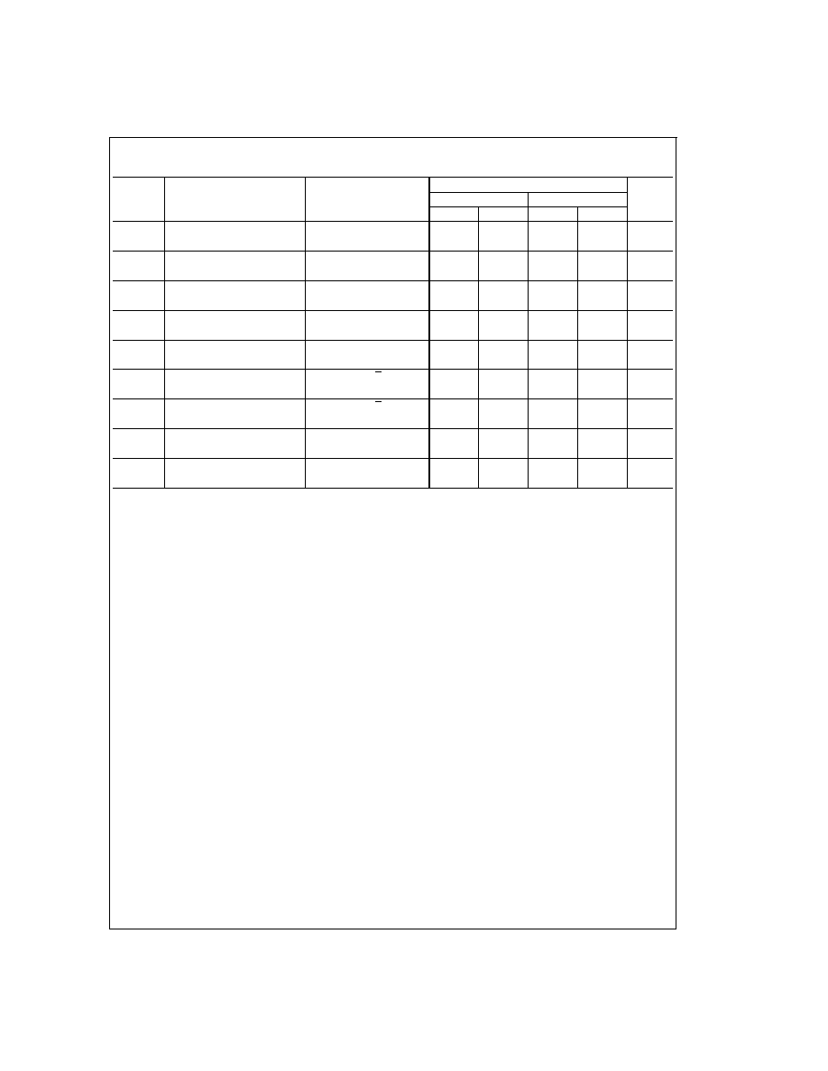
Electrical Characteristics
over recommended operating free air temperature range (unless otherwise noted)
Symbol
Parameter
Conditions
Min
Typ
Max
Units
(Note 5)
V
I
Input Clamp Voltage
V
CC
= Min, I
I
= -18 mA
-1.5
V
V
OH
High Level Output
V
CC
= Min, I
OH
= Max
DM54
2.5
3.4
V
Voltage
V
IL
= Max, V
IH
= Min
DM74
2.7
3.4
V
OL
Low Level Output
V
CC
= Min, I
OL
= Max
DM54
0.25
0.4
Voltage
V
IL
= Max, V
IH
= Min
DM74
0.35
0.5
V
I
OL
= 4 mA, V
CC
= Min
DM74
0.25
0.4
I
I
Input Current
@
Max
V
CC
= Max
Enable T
0.2
mA
Input Voltage
V
I
= 7V
Others
0.1
I
IH
High Level Input
V
CC
= Max
Enable T
40
µA
Current
V
I
= 2.7V
Others
20
I
IL
Low Level Input
V
CC
= Max
Enable T
-0.8
mA
Current
V
I
= 0.4V
Others
-0.4
I
OS
Short Circuit
V
CC
= Max
DM54
-20
-100
mA
Output Current
(Note 6)
DM74
-20
-100
I
CC
Supply Current
V
CC
= Max(Note 7)
20
34
mA
Note 5: All typicals are at V
CC
= 5V and T
A
= 25°C.
Note 6: Not more than one output should be shorted at a time, and the duration should not exceed one second.
Note 7: I
CC
is measured after a momentary 4.5V, then ground, is applied to the CLOCK with all other inputs grounded and all the outputs open.
www.fairchildsemi.com
2