August 1986
Revised February 1999
DM74LS191
Sync
hr
o
nous 4-
Bit
Up/
D
o
w
n
Counter
wi
th
M
o
d
e
Cont
r
o
l
© 1999 Fairchild Semiconductor Corporation
DS006405.prf
www.fairchildsemi.com
DM74LS191
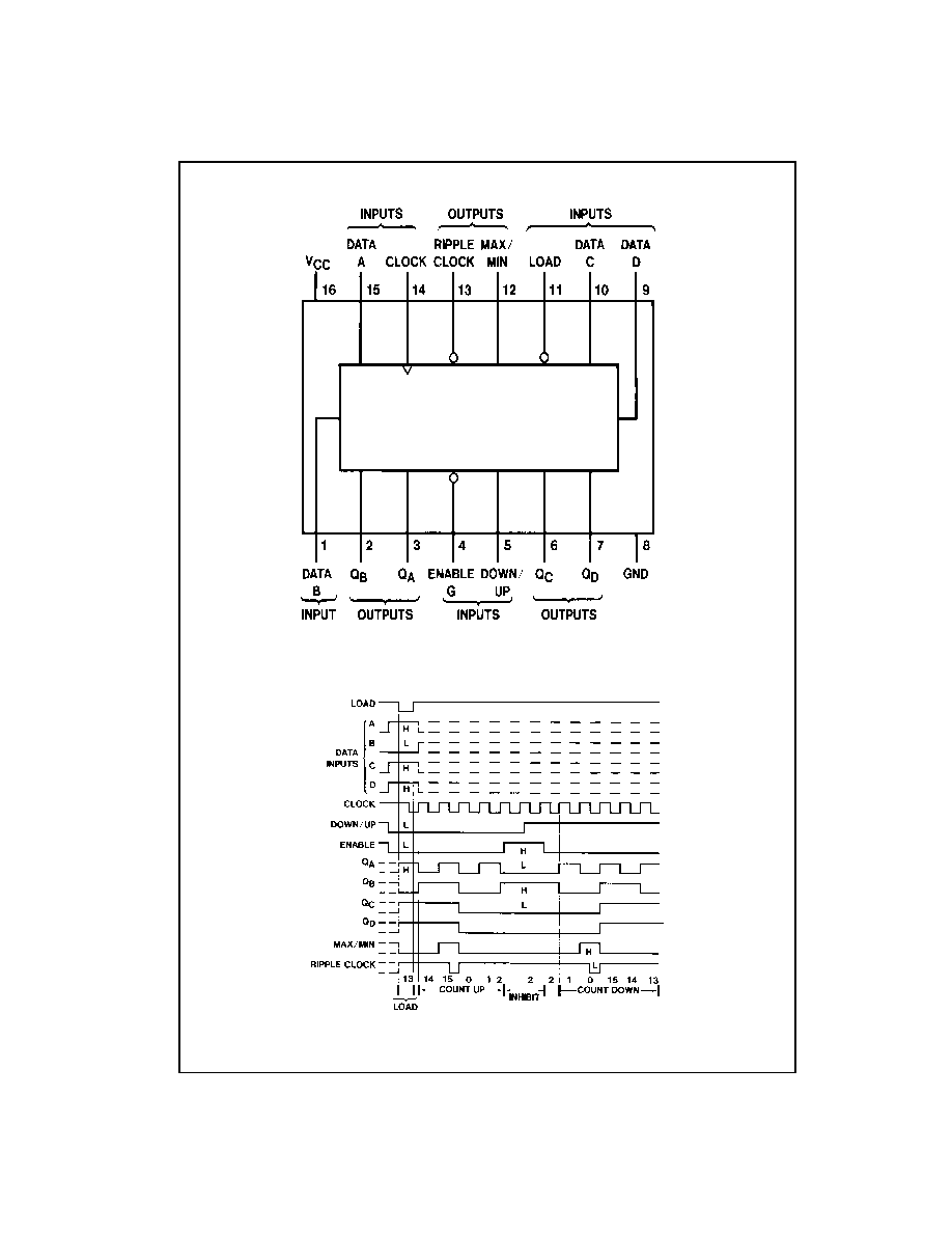
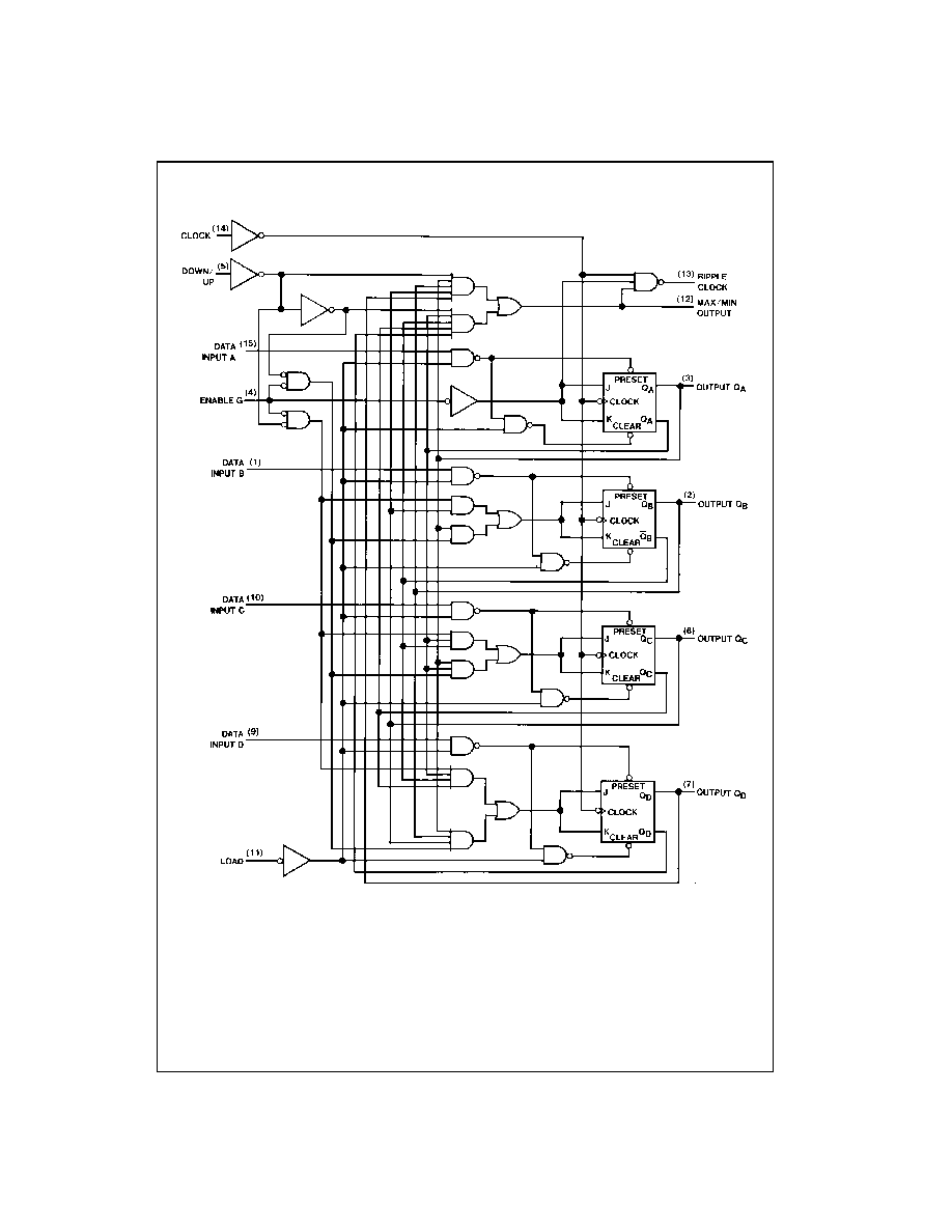
Synchronous 4-Bit Up/Down Counter with Mode Control
General Description
The DM74LS191 circuit is a synchronous, reversible, up/
down counter. Synchronous operation is provided by hav-
ing all flip-flops clocked simultaneously, so that the outputs
change simultaneously when so instructed by the steering
logic. This mode of operation eliminates the output count-
ing spikes normally associated with asynchronous (ripple
clock) counters.
The outputs of the four master-slave flip-flops are triggered
on a LOW-to-HIGH level transition of the clock input, if the
enable input is LOW. A HIGH at the enable input inhibits
counting. Level changes at either the enable input or the
down/up input should be made only when the clock input is
HIGH. The direction of the count is determined by the level
of the down/up input. When LOW, the counter counts up
and when HIGH, it counts down.
The counter is fully programmable; that is, the outputs may
be preset to either level by placing a LOW on the load input
and entering the desired data at the data inputs. The output
will change independent of the level of the clock input. This
feature allows the counters to be used as modulo-N divid-
ers by simply modifying the count length with the preset
inputs.
The clock, down/up, and load inputs are buffered to lower
the drive requirement; which significantly reduces the num-
ber of clock drivers, etc., required for long parallel words.
Two outputs have been made available to perform the cas-
cading function: ripple clock and maximum/minimum count.
The latter output produces a high-level output pulse with a
duration approximately equal to one complete cycle of the
clock when the counter overflows or underflows. The ripple
clock output produces a low-level output pulse equal in
width to the low-level portion of the clock input when an
overflow or underflow condition exists. The counters can be
easily cascaded by feeding the ripple clock output to the
enable input of the succeeding counter if parallel clocking
is used, or to the clock input if parallel enabling is used.
The maximum/minimum count output can be used to
accomplish look-ahead for high-speed operation.
Features
s
Counts binary
s
Single down/up count control line
s
Count enable control input
s
Ripple clock output for cascading
s
Asynchronously presettable with load control
s
Parallel outputs
s
Cascadable for n-bit applications
s
Average propagation delay 20 ns
s
Typical clock frequency 25 MHz
s
Typical power dissipation 100 mW
Ordering Code:
Devices also available in Tape and Reel. Specify by appending the suffix letter "X" to the ordering code.
Order Number
Package Number
Package Description
DM74LS191M
M16A
16-Lead Small Outline Integrated Circuit (SOIC), JEDEC MS-012, 0.150" Narrow Body
DM74LS191N
N16E
16-Lead Plastic Dual-In-Line Package (PDIP), JEDEC MS-001, 0.300" Wide
www.fairchildsemi.com
4
DM74LS191
Absolute Maximum Ratings
(Note 1)
Note 1: The "Absolute Maximum Ratings" are those values beyond which
the safety of the device cannot be guaranteed. The device should not be
operated at these limits. The parametric values defined in the Electrical
Characteristics tables are not guaranteed at the absolute maximum ratings.
The "Recommended Operating Conditions" table will define the conditions
for actual device operation.
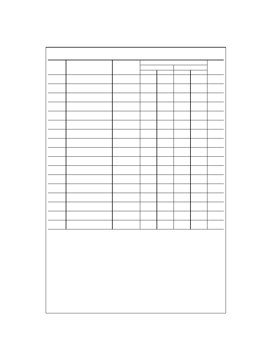
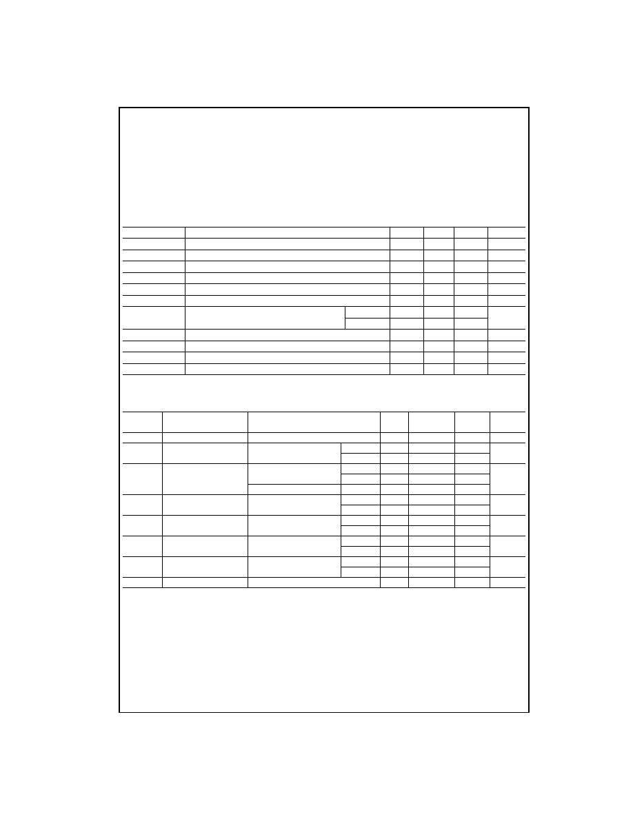
Recommended Operating Conditions
Note 2: T
A
=
25
∞
C and V
CC
=
5V.
DC Electrical Characteristics
Note 3: All typicals are at V
CC
=
5V, T
A
=
25
∞
C.
Note 4: Not more than one output should be shorted at a time, and the duration should not exceed one second.
Note 5: I
CC
is measured with all inputs grounded and all outputs open.
Storage Temperature Range
-
65
∞
C to
+
150
∞
C
Input Voltage
7V
Operating Free Air Temp. Range
0
∞
C to
+
70
∞
C
Supply Voltage
7V
Symbol
Parameter
Min
Nom
Max
Units
V
CC
Supply Voltage
4.75
5
5.25
V
V
IH
HIGH Level Input Voltage
2
V
V
IL
LOW Level Input Voltage
0.8
V
I
OH
HIGH Level Output Current
-
0.4
mA
I
OL
LOW Level Output Current
8
mA
f
CLK
Clock Frequency (Note 2)
0
20
MHz
t
W
Pulse Width
Clock
25
ns
(Note 2)
Load
35
t
SU
Data Setup Time (Note 2)
20
ns
t
H
Data Hold Time (Note 2)
0
ns
t
EN
Enable Time to Clock (Note 2)
30
ns
T
A
Free Air Operating Temperature
0
70
∞
C
Symbol
Parameter
Conditions
Min
Typ
Max
Units
(Note 3)
V
I
Input Clamp Voltage
V
CC
=
Min, I
I
=
-
18 mA
-
1.5
V
V
OH
HIGH
Level Output
V
CC
=
Min, I
OH
=
Max
Mil
2.5
3.4
Voltage
V
IL
=
Max, V
IH
=
Min
Com
2.7
3.4
V
V
OL
LOW
Level Output
V
CC
=
Min, I
OL
=
Max
0.25
0.4
Voltage
V
IL
=
Max, V
IH
=
Min
0.35
0.5
V
I
OL
=
4 mA, V
CC
=
Min
0.25
0.4
I
I
Input Current @ Max
V
CC
=
Max
Enable
0.3
mA
Input Voltage
V
I
=
7V
Others
0.1
I
IH
HIGH
Level Input
V
CC
=
Max
Enable
60
µ
A
Current
V
I
=
2.7V
Others
20
I
IL
LOW
Level Input
V
CC
=
Max
Enable
-
1.08
mA
Current
V
I
=
0.4V
Others
-
0.4
I
OS
Short Circuit
V
CC
=
Max
Mil
-
20
-
100
mA
Output Current
(Note 4)
Com
-
20
-
100
I
CC
Supply Current
V
CC
=
Max (Note 5)
20
35
mA