
© 2000 Fairchild Semiconductor Corporation
DS006407
www.fairchildsemi.com
August 1986
Revised March 2000
DM74LS194
A
4-
B
i
t
Bi
dir
ecti
onal
Uni
versal
Shi
f
t
R
e
gist
er
DM74LS194A
4-Bit Bidirectional Universal Shift Register
General Description
This bidirectional shift register is designed to incorporate
virtually all of the features a system designer may want in a
shift register; they feature parallel inputs, parallel outputs,
right-shift and left-shift serial inputs, operating-mode-con-
trol inputs, and a direct overriding clear line. The register
has four distinct modes of operation, namely:
Parallel (broadside) load
Shift right (in the direction Q
A
toward Q
D
)
Shift left (in the direction Q
D
toward Q
A
)
Inhibit clock (do nothing)
Synchronous parallel loading is accomplished by applying
the four bits of data and taking both mode control inputs,
S0 and S1, HIGH. The data is loaded into the associated
flip-flops and appear at the outputs after the positive transi-
tion of the clock input. During loading, serial data flow is
inhibited.
Shift right is accomplished synchronously with the rising
edge of the clock pulse when S0 is HIGH and S1 is LOW.
Serial data for this mode is entered at the shift-right data
input. When S0 is LOW and S1 is HIGH, data shifts left
synchronously and new data is entered at the shift-left
serial input.
Clocking of the flip-flop is inhibited when both mode control
inputs are LOW.
Features
s
Parallel inputs and outputs
s
Four operating modes:
Synchronous parallel load
Right shift
Left shift
Do nothing
s
Positive edge-triggered clocking
s
Direct overriding clear
Ordering Code:
Devices also available in Tape and Reel. Specify by appending the suffix letter "X" to the ordering code.
Connection Diagram
Order Number
Package Number
Package Description
DM74LS194AM
M16A
16-Lead Small Outline Integrated Circuit (SOIC), JEDEC MS-012, 0.150 Narrow
DM74LS194AN
N16E
16-Lead Plastic Dual-In-Line Package (PDIP), JEDEC MS-001, 0.300 Wide

www.fairchildsemi.com
2
D
M
74LS19
4A
Function Table
H
=
HIGH Level (steady state)
L
=
LOW Level (steady state)
X
=
Don't Care (any input, including transitions)
=
Transition from LOW-to-HIGH level
a, b, c, d
=
The level of steady state input at inputs A, B, C or D, respectively.
Q
A0
, Q
B0
, Q
C0
, Q
D0
=
The level of Q
A
, Q
B
, Q
C
, or Q
D
, respectively, before the indicated steady state input conditions were established.
Q
An
, Q
Bn
, Q
Cn
, Q
Dn
=
The level of Q
A
, Q
B
, Q
C
, respectively, before the most-recent
transition of the clock.
Logic Diagram
Inputs
Outputs
Clear
Mode
Clock
Serial
Parallel
Q
A
Q
B
Q
C
Q
D
S1
S0
Left
Right
A
B
C
D
L
X
X
X
X
X
X
X
X
X
L
L
L
L
H
X
X
L
X
X
X
X
X
X
Q
A0
Q
B0
Q
C0
Q
D0
H
H
H
X
X
a
b
c
d
a
b
c
d
H
L
H
X
H
X
X
X
X
H
Q
An
Q
Bn
Q
Cn
H
L
H
X
L
X
X
X
X
L
Q
An
Q
Bn
Q
Cn
H
H
L
H
X
X
X
X
X
Q
Bn
Q
Cn
Q
Dn
H
H
H
L
L
X
X
X
X
X
Q
Bn
Q
Cn
Q
Dn
L
H
L
L
X
X
X
X
X
X
X
Q
A0
Q
B0
Q
C0
Q
D0

3
www.fairchildsemi.com
DM74LS194
A
Absolute Maximum Ratings
(Note 1)
Note 1: The "Absolute Maximum Ratings" are those values beyond which
the safety of the device cannot be guaranteed. The device should not be
operated at these limits. The parametric values defined in the Electrical
Characteristics tables are not guaranteed at the absolute maximum ratings.
The "Recommended Operating Conditions" table will define the conditions
for actual device operation.
Recommended Operating Conditions
Note 2: C
L
=
15 pF, T
A
=
25
∞
C and V
CC
=
5V.
Note 3: C
L
=
50 pF, R
L
=
2 k
, T
A
=
25
∞
C and V
CC
=
5V.
Note 4: T
A
=
25
∞
C and V
CC
=
5V.
Electrical Characteristics
over recommended operating free air temperature range (unless otherwise noted)
Note 5: All typicals are at V
CC
=
5V, T
A
=
25
∞
C.
Note 6: Not more than one output should be shorted at a time, and the duration should not exceed one second.
Note 7: With all outputs open, inputs A through D grounded, and 4.5V applied to S0, S1, CLEAR, and the serial inputs, I
CC
is tested with momentary ground,
then 4.5V applied to CLOCK.
Supply Voltage
7V
Input Voltage
7V
Operating Free Air Temperature Range
0
∞
C to
+
70
∞
C
Storage Temperature Range
-
65
∞
C to
+
150
∞
C
Symbol
Parameter
Min
Nom
Max
Units
V
CC
Supply Voltage
4.75
5
5.25
V
V
IH
HIGH Level Input Voltage
2
V
V
IL
LOW Level Input Voltage
0.8
V
I
OH
HIGH Level Output Current
-
0.4
mA
I
OL
LOW Level Output Current
8
mA
f
CLK
Clock Frequency (Note 2)
0
25
MHz
Clock Frequency (Note 3)
0
20
t
W
Pulse Width
Clock
20
ns
(Note 4)
Clear
20
t
SU
Setup Time
Mode
30
ns
(Note 4)
Data
20
t
H
Hold Time (Note 4)
0
ns
t
REL
Clear Release Time (Note 4)
25
ns
T
A
Free Air Operating Temperature
0
70
∞
C
Symbol
Parameter
Conditions
Min
Typ
Max
Units
(Note 5)
V
I
Input Clamp Voltage
V
CC
=
Min, I
I
=
-
18 mA
-
1.5
V
V
OH
HIGH Level
V
CC
=
Min, I
OH
=
Max
2.7
3.4
V
Output Voltage
V
IL
=
Max, V
IH
=
Min
V
OL
LOW Level
V
CC
=
Min, I
OL
=
Max
0.35
0.5
Output Voltage
V
IL
=
Max, V
IH
=
Min
V
I
OL
=
4 mA, V
CC
=
Min
0.4
I
I
Input Current @ Max Input Voltage
V
CC
=
Max, V
I
=
7V
0.1
mA
I
IH
HIGH Level Input Current
V
CC
=
Max, V
I
=
2.7V
20
µ
A
I
IL
LOW Level Input Current
V
CC
=
Max, V
I
=
0.4V
-
0.4
mA
I
OS
Short Circuit Output Current
V
CC
=
Max (Note 6)
-
20
-
100
mA
I
CC
Supply Current
V
CC
=
Max (Note 7)
15
23
mA
www.fairchildsemi.com
4
D
M
74LS19
4A
Switching Characteristics
at V
CC
=
5V and T
A
=
25
∞
C
Note 8: All typicals are at V
CC
=
5V, T
A
=
25
∞
C.
Note 9: Not more than one output should be shorted at a time, and the duration should not exceed one second.
Note 10: With all outputs open, inputs A through D grounded, and 4.5V applied to S0, S1, CLEAR, and the serial inputs, I
CC
is tested with momentary
ground, then 4.5V applied to CLOCK.
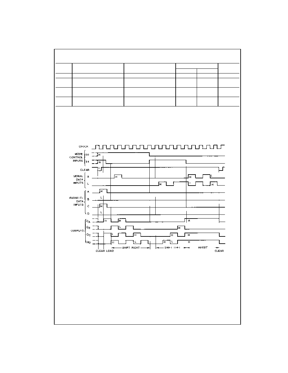
Timing Diagram
Typical Clear, Load, Right-Shift, Left-Shift, Inhibit, and Clear Sequences
Symbol
Parameter
From (Input)
C
L
=
50 pF, R
L
=
2 k
Units
To (Output)
Min
Max
f
MAX
Maximum Clock Frequency
20
MHz
t
PLH
Propagation Delay Time
Clock to Any Q
26
ns
LOW-to-HIGH Level Output
t
PHL
Propagation Delay Time
Clock to Any Q
35
ns
HIGH-to-LOW Level Output
t
PHL
Propagation Delay Time
Clear to Any Q
38
ns
HIGH-to-LOW Output

5
www.fairchildsemi.com
DM74LS194
A
Physical Dimensions
inches (millimeters) unless otherwise noted
16-Lead Small Outline Integrated Circuit (SOIC), JEDEC MS-012, 0.150 Narrow
Package Number M16A