
© 2000 Fairchild Semiconductor Corporation
DS006412
www.fairchildsemi.com
August 1986
Revised January 2000
DM74LS243
Quadrup
le
Bus T
r
anscei
ver
DM74LS243
Quadruple Bus Transceiver
General Description
This four data line transceiver is designed for asynchro-
nous two-way communications between data buses. It can
be used to drive terminated lines down to 133
.
Features
s
Two-way asynchronous communication between data
buses
s
PNP inputs reduce DC loading on bus line
s
Hysteresis at data inputs improves noise margin
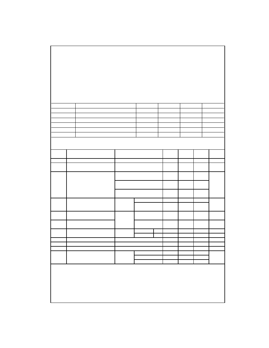
Ordering Code:
Devices also available in Tape and Reel. Specify by appending the suffix letter "X" to the ordering code.
Connection Diagram
Function Table
I
=
Input
O
=
Output
H
=
HIGH Logic Level
L
=
LOW Logic Level
Note 1: Possibly destructive oscillation may occur if the transceivers are
enabled in both directions at once.
Order Number
Package Number
Package Description
DM74LS243M
M14A
14-Lead Small Outline Integrated Circuit (SOIC), JEDEC MS-120, 0.150 Narrow
DM74LS243N
N14A
14-Lead Plastic Dual-In-Line Package (PDIP), JEDEC MS-001, 0.300 Wide
Control
Data Port
Inputs
Status
G AB
GBA
A
B
H
H
O
I
L
H
(Note 1)
(Note 1)
H
L
ISOLATED
L
L
I
O
www.fairchildsemi.com
2
DM74LS243
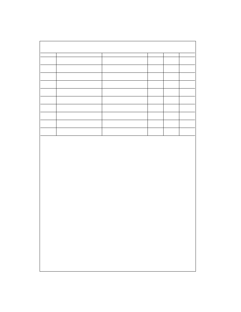
Absolute Maximum Ratings
(Note 2)
Note 2: The "Absolute Maximum Ratings" are those values beyond which
the safety of the device cannot be guaranteed. The device should not be
operated at these limits. The parametric values defined in the Electrical
Characteristics tables are not guaranteed at the absolute maximum ratings.
The "Recommended Operating Conditions" table will define the conditions
for actual device operation.
Recommended Operating Conditions
Electrical Characteristics
over recommended operating free air temperature range (unless otherwise noted)
Note 3: All typicals are at V
CC
=
5V, T
A
=
25
∞
C.
Note 4: Not more than one output should be shorted at a time, and the duration should not exceed one second.
Supply Voltage
7V
Input Voltage
Any G
7V
A or B
5.5V
Operating Free Air Temperature Range
0
∞
C to
+
70
∞
C
Storage Temperature Range
-
65
∞
C to
+
150
∞
C
Symbol
Parameter
Min
Nom
Max
Units
V
CC
Supply Voltage
4.75
5
5.25
V
V
IH
HIGH Level Input Voltage
2
V
V
IL
LOW Level Input Voltage
0.8
V
I
OH
HIGH Level Output Current
-
15
mA
I
OL
LOW Level Output Current
24
mA
T
A
Free Air Operating Temperature
0
70
∞
C
Symbol
Parameter
Conditions Min
Typ
Max
Units
(Note 3)
V
I
Input Clamp Voltage
V
CC
=
Min, I
I
=
-
18 mA
-
1.5
V
HYS
Hysteresis (V
T
+
-
V
T
-
)
V
CC
=
Min
0.2
0.4
V
(Data Inputs Only)
V
OH
HIGH Level Output Voltage
V
CC
=
Min, V
IH
=
Min
2.7
V
IL
=
Max, I
OH
=
-
1 mA
V
CC
=
Min, V
IH
=
Min
2.4
3.4
V
V
IL
=
Max, I
OH
=
-
3 mA
V
CC
=
Min, V
IH
=
Min
2
V
IL
=
0.5V, I
OH
=
Max
V
OL
LOW Level Output Voltage
V
CC
=
Min
I
OL
=
12 mA
0.4
V
IL
=
Max
I
OL
=
Max
V
V
IH
=
Min
0.5
I
OZH
Off-State Output Current,
V
CC
=
Max
V
O
=
2.7V
40
µ
A
HIGH Level Voltage Applied
V
IL
=
Max
I
OZL
Off-State Output Current,
V
IH
=
Min
V
O
=
0.4V
-
200
µ
A
LOW Level Voltage Applied
I
I
Input Current at Maximum
V
CC
=
Max
V
I
=
5.5V
A or B
0.1
mA
Input Voltage
V
I
=
7V
Any G
0.1
mA
I
IH
HIGH Level Input Current
V
CC
=
Max, V
I
=
2.7V
20
µ
A
I
IL
LOW Level Input Current
V
CC
=
Max, V
I
=
0.4V
-
0.2
mA
I
OS
Short Circuit Output Current
V
CC
=
Max (Note 4)
-
40
-
225
mA
I
CC
Supply Current
V
CC
=
Max
Outputs HIGH
22
38
Outputs
Outputs LOW
29
50
mA
OPEN
Outputs Disabled
32
54
3
www.fairchildsemi.com
DM74LS243
Switching Characteristics
at V
CC
=
5V, T
A
=
25
∞
C
Symbol
Parameter
Conditions
Min
Max
Units
t
PLH
Propagation Delay Time
C
L
=
45 pF
18
ns
LOW-to-HIGH Level Output
R
L
=
667
t
PHL
Propagation Delay Time
C
L
=
45 pF
18
ns
HIGH-to-LOW Level Output
R
L
=
667
t
PZL
Output Enable Time
C
L
=
45 pF
30
ns
to LOW Level
R
L
=
667
t
PZH
Output Enable Time
C
L
=
45 pF
23
ns
to HIGH Level
R
L
=
667
t
PLZ
Output Disable Time
C
L
=
5 pF
25
ns
from LOW Level
R
L
=
667
t
PHZ
Output Disable Time
C
L
=
5 pF
18
ns
from HIGH Level
R
L
=
667
t
PLH
Propagation Delay Time
C
L
=
150 pF
21
ns
LOW-to-HIGH Level Output
R
L
=
667
t
PHL
Propagation Delay Time
C
L
=
150 pF
22
ns
HIGH-to-LOW Level Output
R
L
=
667
t
PZL
Output Enable Time
C
L
=
150 pF
33
ns
to LOW Level
R
L
=
667
t
PZH
Output Enable Time
C
L
=
150 pF
26
ns
to HIGH Level
R
L
=
667
www.fairchildsemi.com
4
DM74LS243
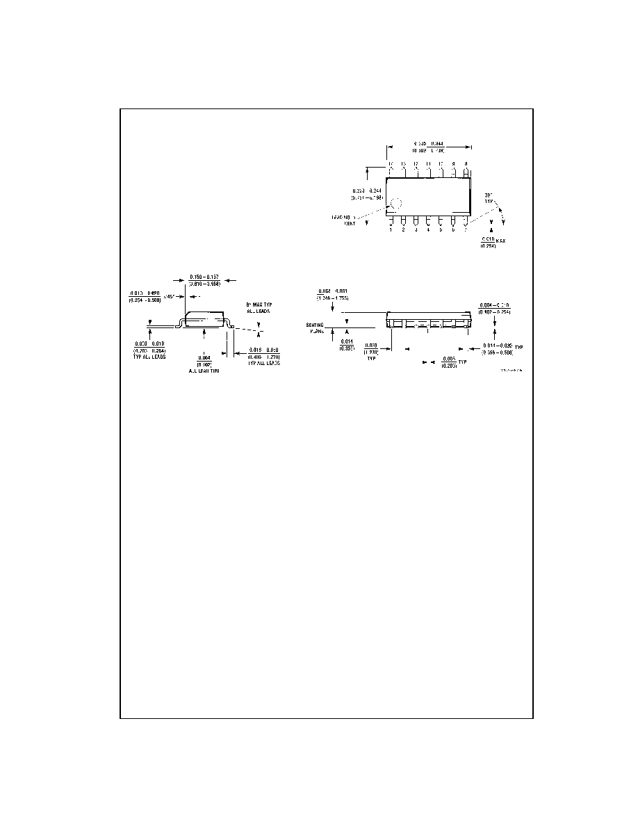
Physical Dimensions
inches (millimeters) unless otherwise noted
14-Lead Small Outline Integrated Circuit (SOIC), JEDEC MS-120, 0.150 Narrow
Package Number M14A
5
www.fairchildsemi.com
DM74LS243
Quadrup
le
Bus T
r
anscei
ver
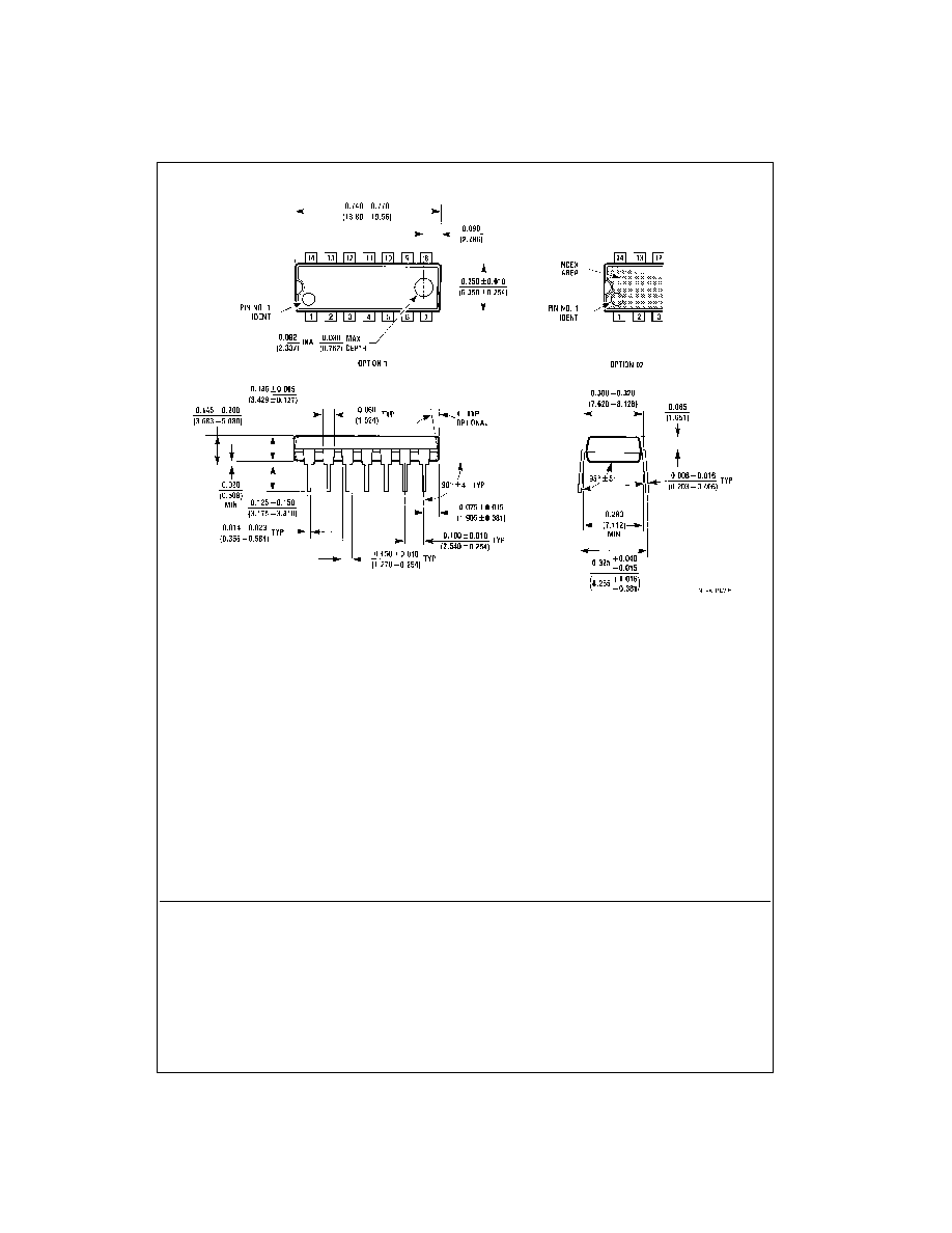
Physical Dimensions
inches (millimeters) unless otherwise noted (Continued)
14-Lead Plastic Dual-In-Line Package (PDIP), JEDEC MS-001, 0.300 Wide
Package Number N14A
Fairchild does not assume any responsibility for use of any circuitry described, no circuit patent licenses are implied and
Fairchild reserves the right at any time without notice to change said circuitry and specifications.
LIFE SUPPORT POLICY
FAIRCHILD'S PRODUCTS ARE NOT AUTHORIZED FOR USE AS CRITICAL COMPONENTS IN LIFE SUPPORT
DEVICES OR SYSTEMS WITHOUT THE EXPRESS WRITTEN APPROVAL OF THE PRESIDENT OF FAIRCHILD
SEMICONDUCTOR CORPORATION. As used herein:
1. Life support devices or systems are devices or systems
which, (a) are intended for surgical implant into the
body, or (b) support or sustain life, and (c) whose failure
to perform when properly used in accordance with
instructions for use provided in the labeling, can be rea-
sonably expected to result in a significant injury to the
user.
2. A critical component in any component of a life support
device or system whose failure to perform can be rea-
sonably expected to cause the failure of the life support
device or system, or to affect its safety or effectiveness.
www.fairchildsemi.com