
© 2000 Fairchild Semiconductor Corporation
DS006416
www.fairchildsemi.com
August 1986
Revised March 2000
DM74LS253
3-
ST
A
T
E Data Selec
t
or
/Mult
i
p
l
exer
DM74LS253
3-STATE Data Selector/Multiplexer
General Description
Each of these Schottky-clamped data selectors/multiplex-
ers contains inverters and drivers to supply fully comple-
mentary, on-chip, binary decoding data selection to the
AND-OR gates. Separate output control inputs are pro-
vided for each of the two four-line sections.
The 3-STATE outputs can interface directly with data lines
of bus-organized systems. With all but one of the common
outputs disabled (at a high impedance state), the low
impedance of the single enabled output will drive the bus
line to a HIGH or LOW logic level.
Features
s
3-STATE version of DM74LS153 with same pinout
s
Schottky-diode-clamped transistors
s
Permit multiplexing from N-lines to one line
s
Performs parallel-to-serial conversion
s
Strobe/output control
s
High fanout totem-pole outputs
s
Typical propagation delay
Data to output
12 ns
Select to output
21 ns
s
Typical power dissipation 35 mW
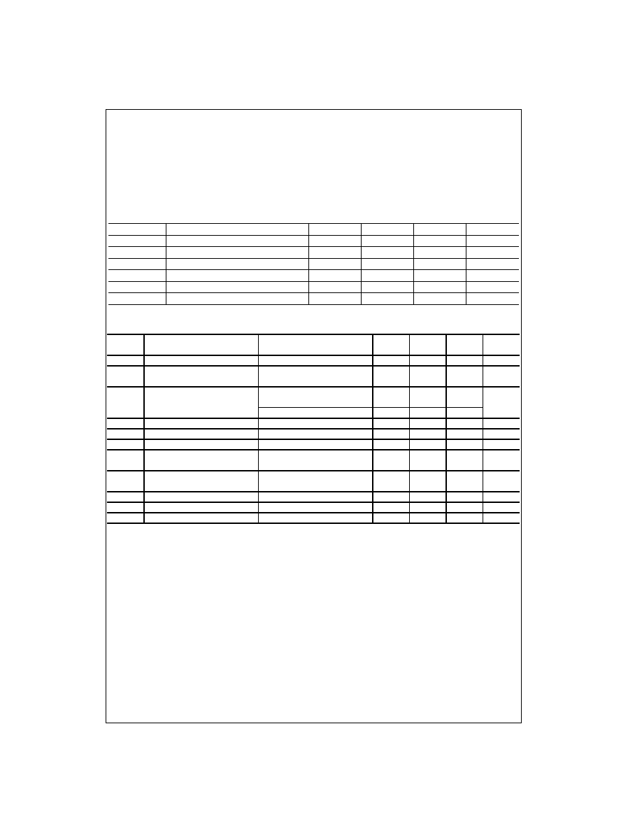
Ordering Code:
Devices also available in Tape and Reel. Specify by appending the suffix letter "X" to the ordering code.
Connection Diagram
Function Table
Address Inputs A and B are common to both sections.
H
=
HIGH Level
L
=
LOW Level
X
=
Don't Care
Z
=
High Impedance (OFF)
Order Number
Package Number
Package Description
DM74LS253M
M16A
16-Lead Small Outline Integrated Circuit (SOIC), JEDEC MS-012, 0.150 Narrow
DM74LS253N
N16E
16-Lead Plastic Dual-In-Line Package (PDIP), JEDEC MS-001, 0.300 Wide
Select
Data Inputs
Output
Output
Inputs
Control
B
A
C0
C1
C2
C3
G
Y
X
X
X
X
X
X
H
Z
L
L
L
X
X
X
L
L
L
L
H
X
X
X
L
H
L
H
X
L
X
X
L
L
L
H
X
H
X
X
L
H
H
L
X
X
L
X
L
L
H
L
X
X
H
X
L
H
H
H
X
X
X
L
L
L
H
H
X
X
X
H
L
H

www.fairchildsemi.com
2
DM74LS253
Logic Diagram
3
www.fairchildsemi.com
DM74LS253
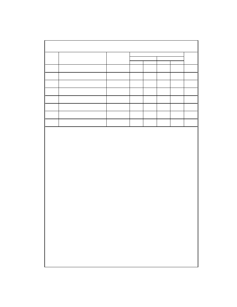
Absolute Maximum Ratings
(Note 1)
Note 1: The "Absolute Maximum Ratings" are those values beyond which
the safety of the device cannot be guaranteed. The device should not be
operated at these limits. The parametric values defined in the "Electrical
Characteristics" table are not guaranteed at the absolute maximum ratings.
The "Recommended Operating Conditions" table will define the conditions
for actual device operation.
Recommended Operating Conditions
Electrical Characteristics
over recommended operating free air temperature range (unless otherwise noted)
Note 2: All typicals are at V
CC
=
5V, T
A
=
25
∞
C.
Note 3: Not more than one output should be shorted at a time, and the duration should not exceed one second.
Note 4: I
CC1
is measured with all outputs OPEN, and all the inputs grounded.
Note 5: I
CC2
is measured with the outputs OPEN, OUTPUT CONTROL at 4.5V and all other inputs grounded.
Supply Voltage
7V
Input Voltage
7V
Operating Free Air Temperature Range
0
∞
C to
+
70
∞
C
Storage Temperature Range
-
65
∞
C to
+
150
∞
C
Symbol
Parameter
Min
Nom
Max
Units
V
CC
Supply Voltage
4.75
5
5.25
V
V
IH
HIGH Level Input Voltage
2
V
V
IL
LOW Level Input Voltage
0.8
V
I
OH
HIGH Level Output Current
-
2.6
mA
I
OL
LOW Level Output Current
24
mA
T
A
Free Air Operating Temperature
0
70
∞
C
Symbol
Parameter
Conditions
Min
Typ
Max
Units
(Note 2)
V
I
Input Clamp Voltage
V
CC
=
Min, I
I
=
-
18 mA
-
1.5
V
V
OH
HIGH Level
V
CC
=
Min, I
OH
=
Max
2.4
3.1
V
Output Voltage
V
IL
=
Max, V
IH
=
Min
V
OL
LOW
Level V
CC
=
Min, I
OL
=
Max
0.5
Output Voltage
V
IL
=
Max, V
IH
=
Min
V
I
OL
=
12 mA, V
CC
=
Min
0.4
I
I
Input Current @ Max Input Voltage
V
CC
=
Max, V
I
=
7V
0.1
mA
I
IH
HIGH Level Input Current
V
CC
=
Max, V
I
=
2.7V
20
µ
A
I
IL
LOW Level Input Current
V
CC
=
Max, V
I
=
0.4V
-
0.4
mA
I
OZH
Off-State Output Current with
V
CC
=
Max, V
O
=
2.7V
20
µ
A
HIGH Level Output Voltage Applied
V
IH
=
Min, V
IL
=
Max
I
OZL
Off-State Output Current with
V
CC
=
Max, V
O
=
0.4
-
20
µ
A
LOW Level Output Voltage Applied
V
IH
=
Min, V
IL
=
Max
I
OS
Short Circuit Output Current
V
CC
=
Max (Note 3)
-
20
-
100
mA
I
CC1
Supply Current
V
CC
=
Max (Note 4)
7
12
mA
I
CC2
Supply Current
V
CC
=
Max (Note 5)
8.5
14
mA
www.fairchildsemi.com
4
DM74LS253
Switching Characteristics
at V
CC
=
5V and T
A
=
25
∞
C
Note 6: C
L
=
5 pF.
From (Input)
R
L
=
667
Symbol
Parameter
To (Output)
C
L
=
45 pF
C
L
=
150 pF
Units
Min
Max
Min
Max
t
PLH
Propagation Delay Time
Data to Y
25
35
ns
LOW-to-HIGH Level Output
t
PHL
Propagation Delay Time
Data to Y
20
30
ns
HIGH-to-LOW Level Output
t
PLH
Propagation Delay Time
Select to Y
45
54
ns
LOW-to-HIGH Level Output
t
PHL
Propagation Delay Time
Select to Y
32
44
ns
HIGH-to-LOW Level Output
t
PZH
Output Enable Time to
Output
18
32
ns
HIGH Level Output
Control to Y
t
PZL
Output Enable Time to
Output
23
35
ns
LOW Level Output
Control to Y
t
PHZ
Output Disable Time from
Output
41
ns
HIGH Level Output (Note 6)
Control to Y
t
PLZ
Output Disable Time from
Output
27
ns
LOW Level Output (Note 6)
Control to Y

5
www.fairchildsemi.com
DM74LS253
Physical Dimensions
inches (millimeters) unless otherwise noted
16-Lead Small Outline Integrated Circuit (SOIC), JEDEC MS-012, 0.150 Narrow
Package Number M16A