 | –≠–ª–µ–∫—Ç—Ä–æ–Ω–Ω—ã–π –∫–æ–º–ø–æ–Ω–µ–Ω—Ç: DM74LS298 | –°–∫–∞—á–∞—Ç—å:  PDF PDF  ZIP ZIP |
© 2000 Fairchild Semiconductor Corporation
DS009826
www.fairchildsemi.com
October 1988
Revised March 2000
DM74LS298
Quad 2-Por
t
Regist
er Mult
ipl
exer
wit
h
S
t
ora
g
e
DM74LS298
Quad 2-Port Register Multiplexer with Storage
General Description
The DM74LS298 is a quad 2-port register. It is the logical
equivalent of a quad 2-input multiplexer followed by a quad
4-bit edge-triggered register. A Common Select input
selects between two 4-bit input ports (data sources). The
selected data is transferred to the output register synchro-
nous with the HIGH-to-LOW transition of the Clock input.
Features
s
Select from two data sources
s
Fully edge-triggered operation
s
Typical power dissipation of 65 mW
Ordering Code:
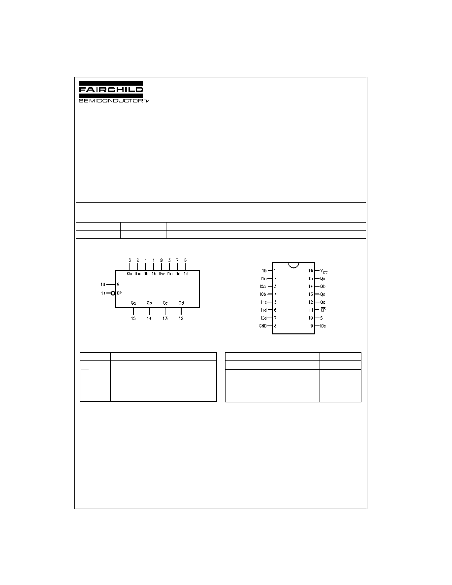
Logic Symbol
V
CC
=
Pin 16
GND
=
Pin 8
Pin Descriptions
Connection Diagram
Truth Table
l
=
LOW Voltage Level one setup time prior to the HIGH-to-LOW clock
transition.
h
=
HIGH Voltage Level one setup time prior to the HIGH-to-LOW clock
transition.
H
=
HIGH Voltage Level
L
=
LOW Voltage Level
X
=
Immaterial
Order Number
Package Number
Package Description
DM74LS298N
N16E
16-Lead Plastic Dual-In-Line Package (PDIP), JEDEC MS-001, 0.300 Wide
Pin Names
Description
S
Common Select Inputs
CP
Clock Pulse Input (Active Falling Edge)
I0
a
, I0
d
Source 0 Data Inputs
I1
a
, I1
d
Source 1 Data Inputs
Q
a
, Q
d
Flip-Flip Outputs
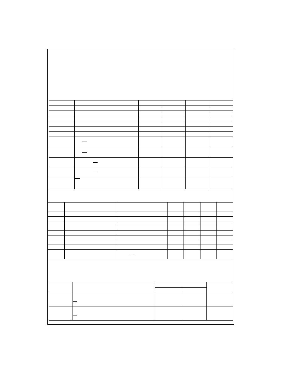
Inputs
Output
S
I0
x
I1
x
Q
x
l
l
X
L
l
h
X
H
h
X
l
L
h
X
h
H

www.fairchildsemi.com
2
DM74LS298
Functional Description
This device is a high speed quad 2-port register. It selects four bits of data from two sources (ports) under the control of a
Common Select input (S). The selected data is transferred to the 4-bit output register synchronous with the HIGH-to-LOW
transition of the Clock input (CP). The 4-bit output register is fully edge-triggered. The Data inputs (I
nx
) and Select input (S)
need be stable only one setup time prior to the HIGH-to-LOW transition of the clock for predictable operation.
Logic Diagram
3
www.fairchildsemi.com
DM74LS298
Absolute Maximum Ratings
(Note 1)
Note 1: The "Absolute Maximum Ratings" are those values beyond which
the safety of the device cannot be guaranteed. The device should not be
operated at these limits. The parametric values defined in the Electrical
Characteristics tables are not guaranteed at the absolute maximum ratings.
The "Recommended Operating Conditions" table will define the conditions
for actual device operation.
Recommended Operating Conditions
Electrical Characteristics
over recommended operating free air temperature range (unless otherwise noted)
Note 2: All typicals are at V
CC
=
5V, T
A
=
25
∞
C.
Note 3: Not more than one output should be shorted at a time, and the duration should not exceed one second.
Switching Characteristics
at V
CC
=
+
5V and T
A
=
+
25
∞
C
Supply Voltage
7V
Input Voltage
7V
Operating Free Air Temperature Range
0
∞
C to
+
70
∞
C
Storage Temperature Range
-
65
∞
C to
+
150
∞
C
Symbol
Parameter
Min
Nom
Max
Units
V
CC
Supply Voltage
4.75
5
5.25
V
V
IH
HIGH Level Input Voltage
2
V
V
IL
LOW Level Input Voltage
0.8
V
I
OH
HIGH Level Output Current
-
0.4
mA
I
OL
LOW Level Output Current
8
mA
T
A
Free Air Operating Temperature
0
70
∞
C
t
S
(H)
Setup Time HIGH or LOW
25
ns
t
S
(L)
S to CP
25
t
H
(H)
Hold Time HIGH or LOW
0
ns
t
H
(L)
S to CP
0
t
S
(H)
Setup Time HIGH or LOW
15
ns
t
S
(L)
I0
x
or I1
x
to CP
15
t
H
(H)
Hold Time HIGH or LOW
5.0
ns
t
H
(L)
I0
x
or I1
x
to CP
5.0
t
W
(H)
CP Pulse Width HIGH or LOW
20
ns
t
W
(L)
20
Symbol
Parameter
Conditions
Min
Typ
Max
Units
(Note 2)
V
I
Input Clamp Voltage
V
CC
=
Min, I
I
=
-
18 mA
-
1.5
V
V
OH
HIGH Level Output Voltage
V
CC
=
Min, I
OH
=
Max, V
IL
=
Max
2.7
3.4
V
V
OL
LOW Level Output Voltage
V
CC
=
Min, I
OL
=
Max, V
IH
=
Min
0.35
0.5
V
I
OL
=
4 mA, V
CC
=
Min
0.25
0.4
I
I
Input Current @ Max Input Voltage
V
CC
=
Max, V
I
=
7V, V
I
=
10V
0.1
mA
I
IH
HIGH Level Input Current
V
CC
=
Max, V
I
=
2.7V
20
µ
A
I
IL
LOW Level Input Current
V
CC
=
Max, V
I
=
0.4V
-
0.4
mA
I
OS
Short Circuit Output Current
V
CC
=
Max (Note 3)
-
20
-
100
mA
I
CC
Supply Current
V
CC
=
Max, I0
n
, I1
n
,
21
mA
S
=
GND, CP
=
Symbol
Parameter
R
L
=
2 k
, C
L
=
15 pF
Units
Min
Max
t
PLH
Propagation Delay Time
LOW-to-HIGH Level Output
25
ns
CP to Q
n
t
PHL
Propagation Delay Time
HIGH-to-LOW Level Output
25
ns
CP to Q
n

www.fairchildsemi.com
4
DM74LS298 Quad 2-Port
R
e
gist
er Mult
ipl
exer wit
h
St
orage
Physical Dimensions
inches (millimeters) unless otherwise noted
16-Lead Plastic Dual-In-Line Package (PDIP), JEDEC MS-001, 0.300 Wide
Package Number N16E
Fairchild does not assume any responsibility for use of any circuitry described, no circuit patent licenses are implied and
Fairchild reserves the right at any time without notice to change said circuitry and specifications.
LIFE SUPPORT POLICY
FAIRCHILD'S PRODUCTS ARE NOT AUTHORIZED FOR USE AS CRITICAL COMPONENTS IN LIFE SUPPORT
DEVICES OR SYSTEMS WITHOUT THE EXPRESS WRITTEN APPROVAL OF THE PRESIDENT OF FAIRCHILD
SEMICONDUCTOR CORPORATION. As used herein:
1. Life support devices or systems are devices or systems
which, (a) are intended for surgical implant into the
body, or (b) support or sustain life, and (c) whose failure
to perform when properly used in accordance with
instructions for use provided in the labeling, can be rea-
sonably expected to result in a significant injury to the
user.
2. A critical component in any component of a life support
device or system whose failure to perform can be rea-
sonably expected to cause the failure of the life support
device or system, or to affect its safety or effectiveness.
www.fairchildsemi.com