 | –≠–ª–µ–∫—Ç—Ä–æ–Ω–Ω—ã–π –∫–æ–º–ø–æ–Ω–µ–Ω—Ç: DM74LS390 | –°–∫–∞—á–∞—Ç—å:  PDF PDF  ZIP ZIP |
© 2000 Fairchild Semiconductor Corporation
DS006433
www.fairchildsemi.com
August 1986
Revised March 2000
DM74LS390
Dual
4-
Bit
Deca
de Count
er
DM74LS390
Dual 4-Bit Decade Counter
General Description
Each of these monolithic circuits contains eight master-
slave flip-flops and additional gating to implement two indi-
vidual four-bit counters in a single package. The
DM74LS390 incorporates dual divide-by-two and divide-
by-five counters, which can be used to implement cycle
lengths equal to any whole and/or cumulative multiples of 2
and/or 5 up to divide-by-100. When connected as a bi-qui-
nary counter, the separate divide-by-two circuit can be
used to provide symmetry (a square wave) at the final out-
put stage. The DM74LS390 has parallel outputs from each
counter stage so that any submultiple of the input count fre-
quency is available for system-timing signals.
Features
s
Dual version of the popular DM74LS90
s
DM74LS390...individual clocks for A and B flip-flops
provide dual
˜
2 and
˜
5 counters
s
Direct clear for each 4-bit counter
s
Dual 4-bit version can significantly improve system den-
sities by reducing counter package count by 50%
s
Typical maximum count frequency...35 MHz
s
Buffered outputs reduce possibility of collector commu-
tation
Ordering Code:
Devices also available in Tape and Reel. Specify by appending the suffix letter "X" to the ordering code.
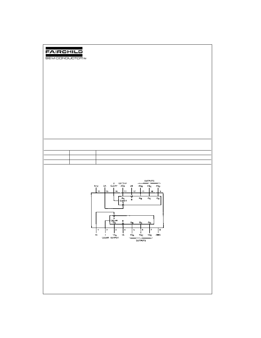
Connection Diagram
Order Number
Package Number
Package Description
DM74LS390M
M16A
16-Lead Small Outline Integrated Circuit (SOIC), JEDEC MS-012, 0.150 Narrow
DM74LS390N
N16E
16-Lead Plastic Dual-In-Line Package (PDIP), JEDEC MS-001, 0.300 Wide
www.fairchildsemi.com
2
DM74LS390
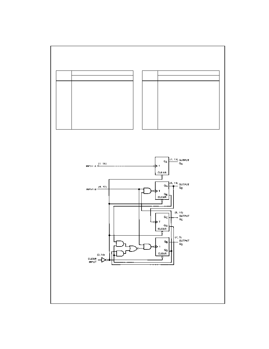
Function Tables
BCD Count Sequence
(Each Counter) (Note 1)
Bi-Quinary (5-2)
(Each Counter) (Note 2)
H
=
HIGH Level
L
=
LOW Level
Note 1: Output Q
A
is connected to input B for BCD count.
Note 2: Output Q
D
is connected to input A for Bi-quinary count.
Logic Diagram
Count
Outputs
Q
D
Q
C
Q
B
Q
A
0
L
L
L
L
1
L
L
L
H
2
L
L
H
L
3
L
L
H
H
4
L
H
L
L
5
L
H
L
H
6
L
H
H
L
7
L
H
H
H
8
H
L
L
L
9
H
L
L
H
Count
Outputs
Q
A
Q
D
Q
C
Q
B
0
L
L
L
L
1
L
L
L
H
2
L
L
H
L
3
L
L
H
H
4
L
H
L
L
5
H
L
L
L
6
H
L
L
H
7
H
L
H
L
8
H
L
H
H
9
H
H
L
L
3
www.fairchildsemi.com
DM74LS390
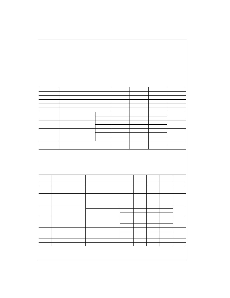
Absolute Maximum Ratings
(Note 3)
Note 3: The "Absolute Maximum Ratings" are those values beyond which
the safety of the device cannot be guaranteed. The device should not be
operated at these limits. The parametric values defined in the Electrical
Characteristics tables are not guaranteed at the absolute maximum ratings.
The "Recommended Operating Conditions" table will define the conditions
for actual device operation.
Recommended Operating Conditions
Note 4: C
L
=
15 pF, R
L
=
2 k
, T
A
=
25
∞
C and V
CC
=
5V.
Note 5: C
L
=
50 pF, R
L
=
2 k
, T
A
=
25
∞
C and V
CC
=
5V.
Note 6: The symbol (
) indicates the falling edge of the clear pulse is used for reference.
Note 7: T
A
=
25
∞
C and V
CC
=
5V.
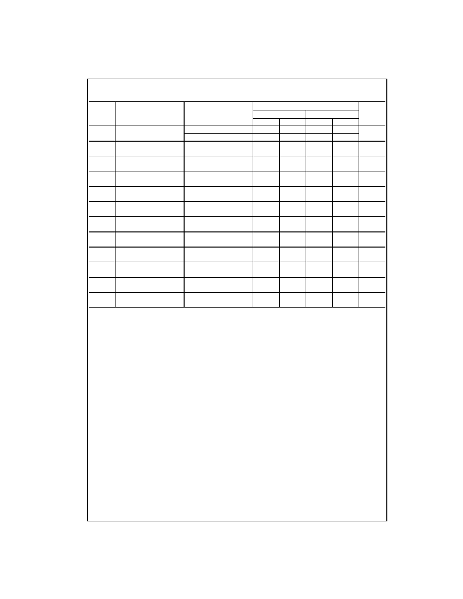
Electrical Characteristics
over recommended operating free air temperature range (unless otherwise noted)
Note 8: All typicals are at V
CC
=
5V, T
A
=
25
∞
C.
Note 9: Not more than one output should be shorted at a time, and the duration should not exceed one second.
Note 10: I
CC
is measured with all outputs OPEN, both CLEAR inputs grounded following momentary connection to 4.5 and all other inputs grounded.
Supply Voltage
7V
Input Voltage
Clear
7V
A or B
5.5V
Operating Free Air Temperature Range
0
∞
C to
+
70
∞
C
Storage Temperature Range
-
65
∞
C to
+
150
∞
C
Symbol
Parameter
Min
Nom
Max
Units
V
CC
Supply Voltage
4.75
5
5.25
V
V
IH
HIGH Level Input Voltage
2
V
V
IL
LOW Level Input Voltage
0.8
V
I
OH
HIGH Level Output Current
-
0.4
mA
I
OL
LOW Level Output Current
8
mA
f
CLK
Clock Frequency (Note 4)
A to Q
A
0
25
MHz
B to Q
B
0
20
f
CLK
Clock Frequency (Note 5)
A to Q
A
0
20
MHz
B to Q
B
0
15
t
W
Pulse Width (Note 4)
A
20
B
25
ns
Clear HIGH
20
t
REL
Clear Release Time (Note 6)(Note 7)
25
ns
T
A
Free Air Operating Temperature
0
70
∞
C
Symbol
Parameter
Conditions
Min
Typ
Max
Units
(Note 8)
V
I
Input Clamp Voltage
V
CC
=
Min, I
I
=
-
18 mA
-
1.5
V
V
OH
HIGH Level
V
CC
=
Min, I
OH
=
Max
2.7
3.4
V
Output Voltage
V
IL
=
Max, V
IH
=
Min
V
OL
LOW
Level V
CC
=
Min, I
OL
=
Max
0.35
0.5
Output Voltage
V
IL
=
Max, V
IH
=
Min
V
I
OL
=
4 mA, V
CC
=
Min
0.25
0.4
I
I
Input Current @ Max
V
CC
=
Max, V
I
=
7V
Clear
0.1
Input Voltage
V
CC
=
Max
A
0.2
mA
V
I
=
5.5V
B
0.4
I
IH
HIGH Level
V
CC
=
Max
Clear
20
Input Current
V
I
=
2.7V
A
40
µ
A
B
80
I
IL
LOW
Level V
CC
=
Max, V
I
=
0.4V
Clear
-
0.4
Input Current
A
-
1.6
mA
B
-
2.4
I
OS
Short Circuit Output Current
V
CC
=
Max (Note 9)
-
20
-
100
mA
I
CC
Supply Current
V
CC
=
Max (Note 10)
15
26
mA
www.fairchildsemi.com
4
DM74LS390
Switching Characteristics
at V
CC
=
5V and T
A
=
25
∞
C
R
L
=
2 k
Symbol
Parameter
From (Input)
C
L
=
15 pF
C
L
=
50 pF
Units
To (Output)
Min
Max
Min
Max
f
MAX
Maximum Clock
A to Q
A
25
20
MHz
Frequency
B to Q
B
20
15
t
PLH
Propagation Delay Time
A to Q
A
20
24
ns
LOW-to-HIGH Level Output
t
PHL
Propagation Delay Time
A to Q
A
20
30
ns
HIGH-to-LOW Level Output
t
PLH
Propagation Delay Time
A to Q
C
60
81
ns
LOW-to-HIGH Level Output
t
PHL
Propagation Delay Time
A to Q
C
60
81
ns
HIGH-to-LOW Level Output
t
PLH
Propagation Delay Time
B to Q
B
21
27
ns
LOW-to-HIGH Level Output
t
PHL
Propagation Delay Time
B to Q
B
21
33
ns
HIGH-to-LOW Level Output
t
PLH
Propagation Delay Time
B to Q
C
39
51
ns
LOW-to-HIGH Level Output
t
PHL
Propagation Delay Time
B to Q
C
39
54
ns
HIGH-to-LOW Level Output
t
PLH
Propagation Delay Time
B to Q
D
21
27
ns
LOW-to-HIGH Level Output
t
PHL
Propagation Delay Time
B to Q
D
21
33
ns
HIGH-to-LOW Level Output
t
PHL
Propagation Delay Time
Clear to Any Q
39
45
ns
HIGH-to-LOW Level Output
5
www.fairchildsemi.com
DM74LS390
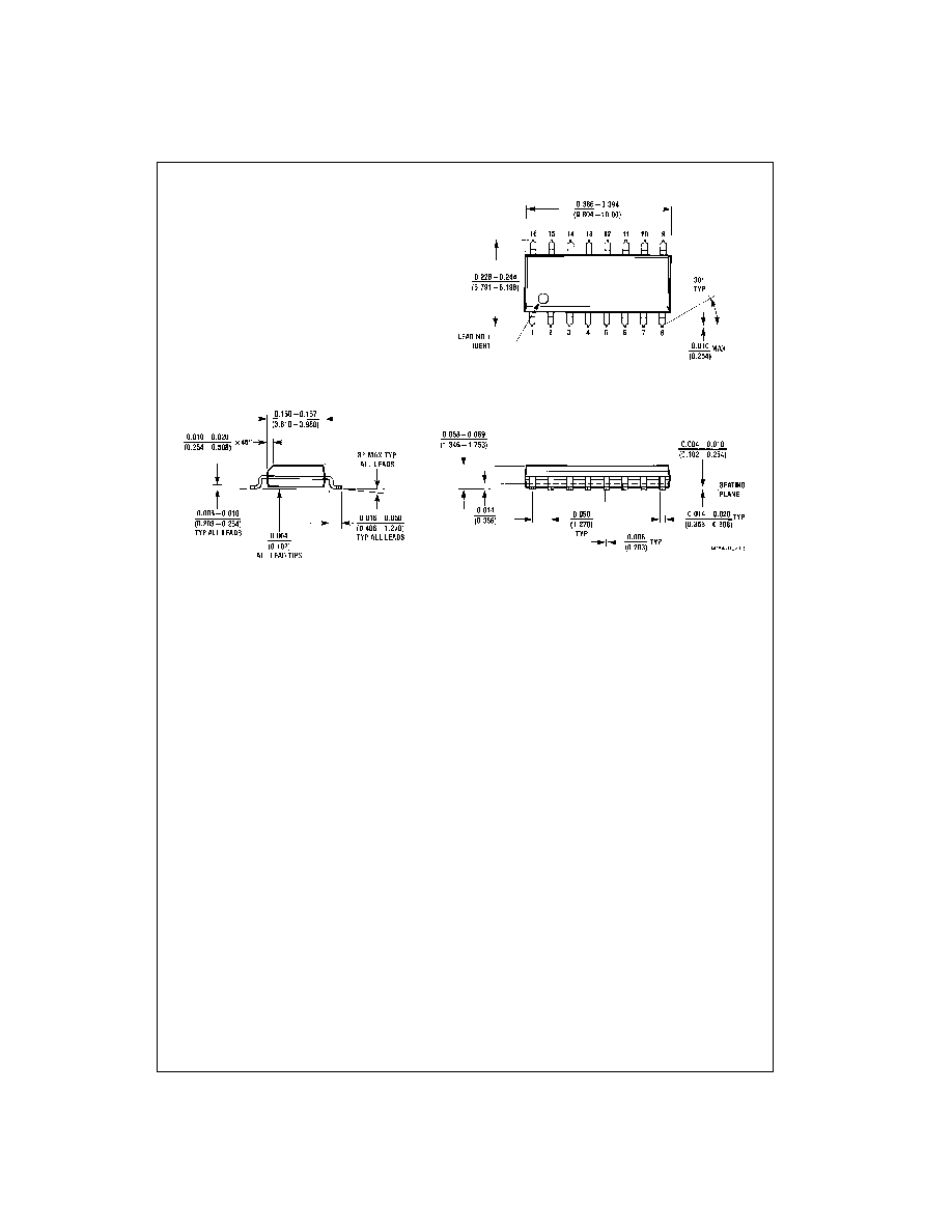
Physical Dimensions
inches (millimeters) unless otherwise noted
16-Lead Small Outline Integrated Circuit (SOIC), JEDEC MS-012, 0.150 Narrow
Package Number M16A