 | –≠–ª–µ–∫—Ç—Ä–æ–Ω–Ω—ã–π –∫–æ–º–ø–æ–Ω–µ–Ω—Ç: DM74LS90 | –°–∫–∞—á–∞—Ç—å:  PDF PDF  ZIP ZIP |
© 2000 Fairchild Semiconductor Corporation
DS006381
www.fairchildsemi.com
August 1986
Revised March 2000
DM74LS90 Decade and Binar
y
Count
ers
DM74LS90
Decade and Binary Counters
General Description
Each of these monolithic counters contains four master-
slave flip-flops and additional gating to provide a divide-by-
two counter and a three-stage binary counter for which the
count cycle length is divide-by-five for the DM74LS90.
All of these counters have a gated zero reset and the
DM74LS90 also has gated set-to-nine inputs for use in
BCD nine's complement applications.
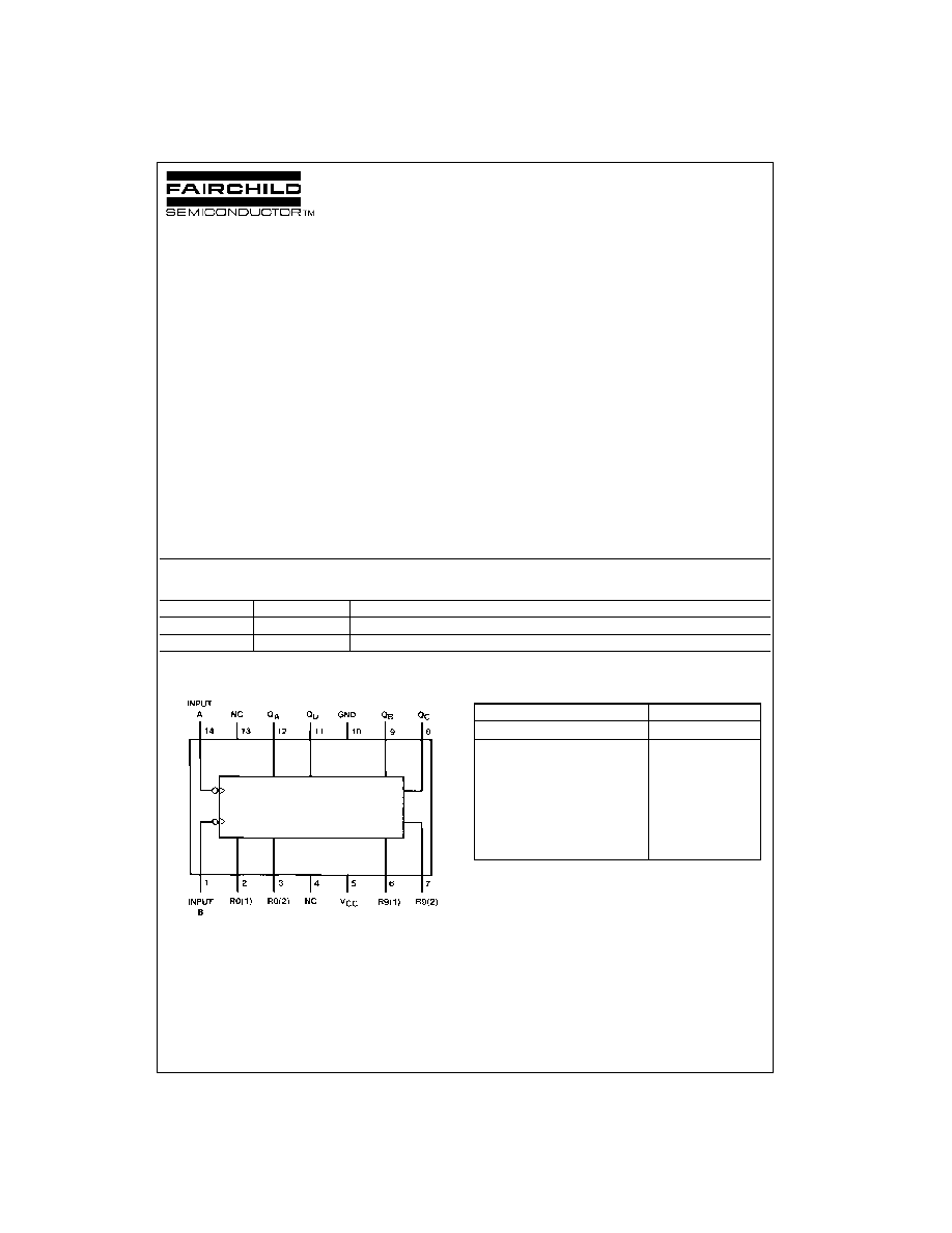
To use their maximum count length (decade or four bit
binary), the B input is connected to the Q
A
output. The
input count pulses are applied to input A and the outputs
are as described in the appropriate truth table. A symmetri-
cal divide-by-ten count can be obtained from the
DM74LS90 counters by connecting the Q
D
output to the A
input and applying the input count to the B input which
gives a divide-by-ten square wave at output Q
A
.
Features
s
Typical power dissipation 45 mW
s
Count frequency 42 MHz
Ordering Code:
Devices also available in Tape and Reel. Specify by appending the suffix letter "X" to the ordering code.
Connection Diagram
Reset/Count Truth Table
Order Number
Package Number
Package Description
DM74LS90M
M14A
14-Lead Small Outline Integrated Circuit (SOIC), JEDEC MS-120, 0.150 Narrow
DM74LS90N
N14A
14-Lead Plastic Dual-In-Line Package (PDIP), JEDEC MS-001, 0.300 Wide
Reset Inputs
Output
R0(1)
R0(2)
R9(1)
R9(2)
Q
D
Q
C
Q
B
Q
A
H
H
L
X
L
L
L
L
H
H
X
L
L
L
L
L
X
X
H
H
H
L
L
H
X
L
X
L
COUNT
L
X
L
X
COUNT
L
X
X
L
COUNT
X
L
L
X
COUNT
www.fairchildsemi.com
2
D
M
74LS90
Function Tables
BCD Count Sequence (Note 1)
Bi-Quinary (5-2) (Note 2)
H
=
HIGH Level
L
=
LOW Level
X
=
Don't Care
Note 1: Output Q
A
is connected to input B for BCD count.
Note 2: Output Q
D
is connected to input A for bi-quinary count.
Note 3: Output Q
A
is connected to input B.
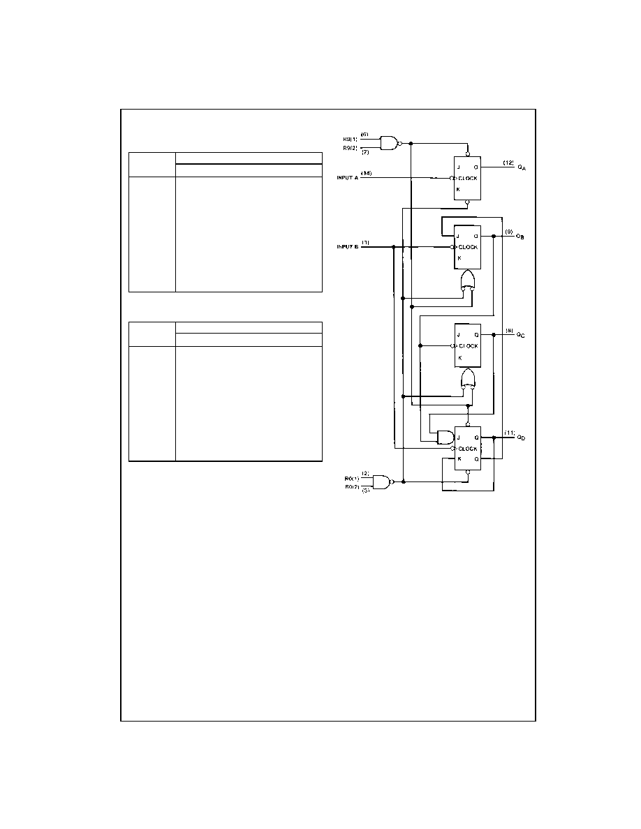
Logic Diagram
The J and K inputs shown without connection are for reference only and
are functionally at a high level.
Count
Output
Q
D
Q
C
Q
B
Q
A
0
L
L
L
L
1
L
L
L
H
2
L
L
H
L
3
L
L
H
H
4
L
H
L
L
5
L
H
L
H
6
L
H
H
L
7
L
H
H
H
8
H
L
L
L
9
H
L
L
H
Count
Output
Q
A
Q
D
Q
C
Q
B
0
L
L
L
L
1
L
L
L
H
2
L
L
H
L
3
L
L
H
H
4
L
H
L
L
5
H
L
L
L
6
H
L
L
H
7
H
L
H
L
8
H
L
H
H
9
H
H
L
L
3
www.fairchildsemi.com
DM74LS90
Absolute Maximum Ratings
(Note 4)
Note 4: The "Absolute Maximum Ratings" are those values beyond which
the safety of the device cannot be guaranteed. The device should not be
operated at these limits. The parametric values defined in the "Electrical
Characteristics" table are not guaranteed at the absolute maximum ratings.
The "Recommended Operating Conditions" table will define the conditions
for actual device operation.
Recommended Operating Conditions
Note 5: C
L
=
15 pF, R
L
=
2 k
, T
A
=
25
∞
C and V
CC
=
5V.
Note 6: C
L
=
50 pF, R
L
=
2 k
, T
A
=
25
∞
C and V
CC
=
5V.
Electrical Characteristics
over recommended operating free air temperature range (unless otherwise noted)
Note 7: All typicals are at V
CC
=
5V, T
A
=
25
∞
C.
Supply Voltage
7V
Input Voltage (Reset)
7V
Input Voltage (A or B)
5.5V
Operating Free Air Temperature Range
0
∞
C to
+
70
∞
C
Storage Temperature Range
-
65
∞
C to
+
150
∞
C
Symbol
Parameter
Min
Nom
Max
Units
V
CC
Supply Voltage
4.75
5
5.25
V
V
IH
HIGH Level Input Voltage
2
V
V
IL
LOW Level Input Voltage
0.8
V
I
OH
HIGH Level Output Current
-
0.4
mA
I
OL
LOW Level Output Current
8
mA
f
CLK
Clock Frequency (Note 5)
A to Q
A
0
32
MHz
B to Q
B
0
16
f
CLK
Clock Frequency (Note 6)
A to Q
A
0
20
MHz
B to Q
B
0
10
t
W
Pulse Width (Note 5)
A
15
B
30
ns
Reset
15
t
W
Pulse Width (Note 6)
A
25
B
50
ns
Reset
25
t
REL
Reset Release Time (Note 5)
25
ns
t
REL
Reset Release Time (Note 6)
35
ns
T
A
Free Air Operating Temperature
0
70
∞
C
Symbol
Parameter
Conditions
Min
Typ
Max
Units
(Note 7)
V
I
Input Clamp Voltage
V
CC
=
Min, I
I
=
-
18 mA
-
1.5
V
V
OH
HIGH Level
V
CC
=
Min, I
OH
=
Max
2.7
3.4
V
Output Voltage
V
IL
=
Max, V
IH
=
Min
V
OL
LOW
Level V
CC
=
Min, I
OL
=
Max
(Note 8)
V
Output Voltage
V
IL
=
Max, V
IH
=
Min
0.35
0.5
I
OL
=
4 mA, V
CC
=
Min
0.25
0.4
I
I
Input Current @ Max
V
CC
=
Max, V
I
=
7V
Reset
0.1
mA
Input Voltage
V
CC
=
Max
A
0.2
V
I
=
5.5V
B
0.4
I
IH
HIGH Level
V
CC
=
Max, V
I
=
2.7V
Reset
20
µ
A
Input Current
A
40
B
80
I
IL
LOW
Level V
CC
=
Max, V
I
=
0.4V
Reset
-
0.4
mA
Input Current
A
-
2.4
B
-
3.2
I
OS
Short Circuit Output Current
V
CC
=
Max (Note 9)
-
20
-
100
mA
I
CC
Supply Current
V
CC
=
Max (Note 7)
9
15
mA
www.fairchildsemi.com
4
D
M
74LS90
Electrical Characteristics
(Continued)
Note 8: Q
A
outputs are tested at I
OL
=
Max plus the limit value of I
IL
for the B input. This permits driving the B input while maintaining full fan-out capability.
Note 9: Not more than one output should be shorted at a time, and the duration should not exceed one second.
Note 10: I
CC
is measured with all outputs open, both RO inputs grounded following momentary connection to 4.5V and all other inputs grounded.
Switching Characteristics
at V
CC
=
5V and T
A
=
25
∞
C
From (Input)
R
L
=
2 k
Symbol
Parameter
To (Output)
C
L
=
15 pF
C
L
=
50 pF
Units
Min
Max
Min
Max
f
MAX
Maximum Clock
A to Q
A
32
20
MHz
Frequency
B to Q
B
16
10
t
PLH
Propagation Delay Time
A to Q
A
16
20
ns
LOW-to-HIGH Level Output
t
PHL
Propagation Delay Time
A to Q
A
18
24
ns
HIGH-to-LOW Level Output
t
PLH
Propagation Delay Time
A to Q
D
48
52
ns
LOW-to-HIGH Level Output
t
PHL
Propagation Delay Time
A to Q
D
50
60
ns
HIGH-to-LOW Level Output
t
PLH
Propagation Delay Time
B to Q
B
16
23
ns
LOW-to-HIGH Level Output
t
PHL
Propagation Delay Time
B to Q
B
21
30
ns
HIGH-to-LOW Level Output
t
PLH
Propagation Delay Time
B to Q
C
32
37
ns
LOW-to-HIGH Level Output
t
PHL
Propagation Delay Time
B to Q
C
35
44
ns
HIGH-to-LOW Level Output
t
PLH
Propagation Delay Time
B to Q
D
32
36
ns
LOW-to-HIGH Level Output
t
PHL
Propagation Delay Time
B to Q
D
35
44
ns
HIGH-to-LOW Level Output
t
PLH
Propagation Delay Time
SET-9 to Q
A
, Q
D
30
35
ns
LOW-to-HIGH Level Output
t
PHL
Propagation Delay Time
SET-9 to Q
B
, Q
C
40
48
ns
HIGH-to-LOW Level Output
t
PHL
Propagation Delay Time
SET-0 to Any Q
40
52
ns
HIGH-to-LOW Level Output

5
www.fairchildsemi.com
DM74LS90
Physical Dimensions
inches (millimeters) unless otherwise noted
14-Lead Small Outline Integrated Circuit (SOIC), JEDEC MS-120, 0.150 Narrow
Package Number M14A