 | –≠–ª–µ–∫—Ç—Ä–æ–Ω–Ω—ã–π –∫–æ–º–ø–æ–Ω–µ–Ω—Ç: DM74S283N | –°–∫–∞—á–∞—Ç—å:  PDF PDF  ZIP ZIP |

© 2000 Fairchild Semiconductor Corporation
DS006484
www.fairchildsemi.com
August 1986
Revised May 2000
DM74S283 4-
Bit
Bi
nary Adder wit
h
Fast
C
a
rry
DM74S283
4-Bit Binary Adder with Fast Carry
General Description
These full adders perform the addition of two 4-bit binary
numbers. The sum (
) outputs are provided for each bit
and the resultant carry (C4) is obtained from the fourth bit.
These adders feature full internal look ahead across all four
bits. This provides the system designer with partial look-
ahead performance at the economy and reduced package
count of a ripple-carry implementation.
The adder logic, including the carry, is implemented in its
true form meaning that the end-around carry can be
accomplished without the need for logic or level inversion.
Features
s
Full-carry look-ahead across the four bits
s
Systems achieve partial look-ahead performance with
the economy of ripple carry
s
Typical add times
Two 8-bit words
15 ns
Two 16-bit words 30 ns
s
Typical power dissipation 510 mW
Ordering Code:
Connection Diagram
Order Number
Package Number
Package Description
DM74S283N
N16E
16-Lead Plastic Dual-In-Line Package (PDIP), JEDEC MS-001, 0.300 Wide

www.fairchildsemi.com
2
D
M
74S283
Function Table
Logic Diagram
H
=
HIGH Level,
L
=
LOW Level
Note: Input conditions at A1, B1, A2, B2, and C0 are used to determine outputs
1 and
2 and the value of the internal carry C2. The values at C2, A3,
B3, A4, and B4 are then used to determine outputs
3,
4, and C4.
3
www.fairchildsemi.com
DM74S283
Absolute Maximum Ratings
(Note 1)
Note 1: The "Absolute Maximum Ratings" are those values beyond which
the safety of the device cannot be guaranteed. The device should not be
operated at these limits. The parametric values defined in the Electrical
Characteristics tables are not guaranteed at the absolute maximum ratings.
The "Recommended Operating Conditions" table will define the conditions
for actual device operation.
Recommended Operating Conditions
Electrical Characteristics
over recommended operating free air temperature (unless otherwise noted)
Note 2: All typicals are at V
CC
=
5V, T
A
=
25
∞
C.
Note 3: Not more than one output should be shorted at a time, and the duration should not exceed one second.
Note 4: I
CC1
is measured with all outputs OPEN, all B inputs LOW and all other inputs at 4.5V.
Note 5: I
CC2
is measured with all outputs OPEN and all inputs at 4.5V.
Supply Voltage
7V
Input Voltage
5.5V
Operating Free Air Temperature Range
0
∞
C to
+
70
∞
C
Storage Temperature Range
-
65
∞
C to
+
150
∞
C
Symbol
Parameter
Min
Nom
Max
Units
V
CC
Supply Voltage
4.75
5
5.25
V
V
IH
HIGH Level Input Voltage
2
V
V
IL
LOW Level Input Voltage
0.8
V
I
OH
HIGH Level Output Current (Output C4)
-
0.5
mA
HIGH Level Output Current (Other Outputs)
-
1
I
OL
LOW Level Output Current (Output C4)
10
mA
LOW Level Output Current (Other Outputs)
20
T
A
Free Air Operating Temperature
0
70
∞
C
Symbol
Parameter
Conditions
Min
Typ
Max
Units
(Note 2)
V
I
Input Clamp Voltage
V
CC
=
Min, I
I
=
-
18 mA
-
1.2
V
V
OH
HIGH Level
V
CC
=
Min, I
OH
=
Max
2.7
3.4
V
Output Voltage
V
IL
=
Max, V
IH
=
Min
V
OL
LOW Level
V
CC
=
Min, I
OL
=
Max
0.5
V
Output Voltage
V
IH
=
Min, V
IL
=
Max
I
I
Input Current @ Max Input Voltage
V
CC
=
Max, V
I
=
5.5V
1
mA
I
IH
HIGH Level Input Current
V
CC
=
Max, V
I
=
2.7V
50
µ
A
I
L
LOW Level Input Current
V
CC
=
Max, V
I
=
0.5V
-
2
mA
I
OS
Short Circuit
V
CC
=
Max
C4 Output
-
20
-
100
mA
Output Current
(Note 3)
Other Outputs
-
40
-
100
I
CC1
Supply Current
V
CC
=
Max (Note 4)
80
120
mA
I
CC2
Supply Current
V
CC
=
Max (Note 5)
95
160
mA

www.fairchildsemi.com
4
D
M
74S283
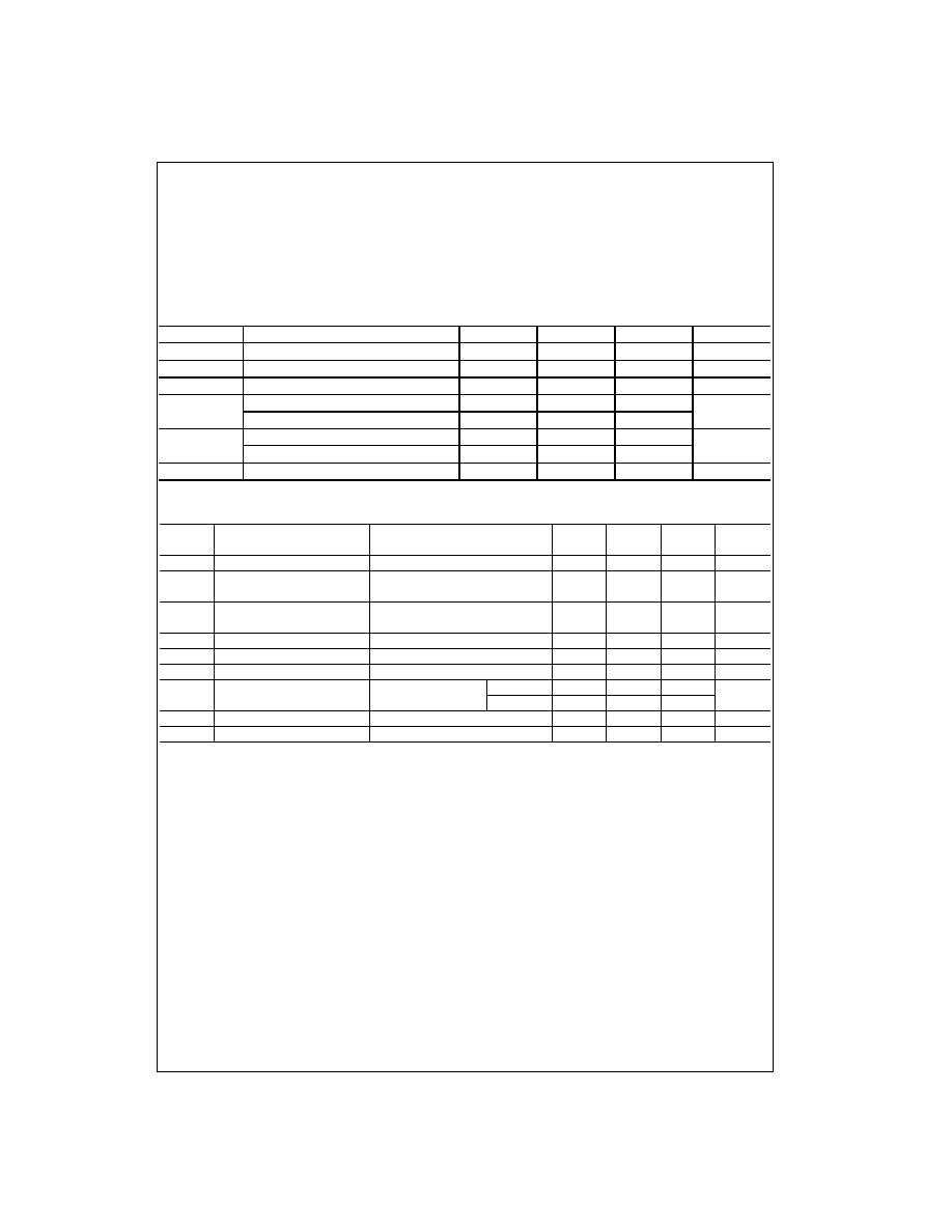
Switching Characteristics
at V
CC
=
5V and T
A
=
25
∞
C
Note 6: R
L
=
560
.
R
L
=
280
Symbol
Parameter
From (Input)
C
L
=
15 pF
C
L
=
50 pF
Units
To (Output)
Min
Max
Min
Max
t
PLH
Propagation Delay Time
C0 to
1 or
2
18
20
ns
LOW-to-HIGH Level Output
t
PHL
Propagation Delay Time
C0 to
1 or
2
18
20
ns
HIGH-to-LOW Level Output
t
PLH
Propagation Delay Time
C0 to
3
18
20
ns
LOW-to-HIGH Level Output
t
PHL
Propagation Delay Time
C0 to
3
18
20
ns
HIGH-to-LOW Level Output
t
PLH
Propagation Delay Time
C0 to
4
18
20
ns
LOW-to-HIGH Level Output
t
PHL
Propagation Delay Time
C0 to
4
18
20
ns
HIGH-to-LOW Level Output
t
PLH
Propagation Delay Time
A
i
, B
i
to S
i
18
20
ns
LOW-to-HIGH Level Output
t
PHL
Propagation Delay Time
A
i
, B
i
to S
i
18
20
ns
HIGH-to-LOW Level Output
t
PLH
Propagation Delay Time
C0 to
4
11
15
ns
LOW-to-HIGH Level Output (Note 6)
t
PHL
Propagation Delay Time
C0 to
4
11
15
ns
HIGH-to-LOW Level Output (Note 6)
t
PLH
Propagation Delay Time
A
i
, B
i
to C4
12
16
ns
LOW-to-HIGH Level Output (Note 6)
t
PHL
Propagation Delay Time
A
i
, B
i
to C4
12
16
ns
HIGH-to-LOW Level Output (Note 6)

5
www.fairchildsemi.com
DM74S283 4-
Bit
Bi
nary Adder wit
h
Fast
C
a
rry
Physical Dimensions
inches (millimeters) unless otherwise noted
16-Lead Plastic Dual-In-Line Package (PDIP), JEDEC MS-001, 0.300 Wide
Package Number N16E
Fairchild does not assume any responsibility for use of any circuitry described, no circuit patent licenses are implied and
Fairchild reserves the right at any time without notice to change said circuitry and specifications.
LIFE SUPPORT POLICY
FAIRCHILD'S PRODUCTS ARE NOT AUTHORIZED FOR USE AS CRITICAL COMPONENTS IN LIFE SUPPORT
DEVICES OR SYSTEMS WITHOUT THE EXPRESS WRITTEN APPROVAL OF THE PRESIDENT OF FAIRCHILD
SEMICONDUCTOR CORPORATION. As used herein:
1. Life support devices or systems are devices or systems
which, (a) are intended for surgical implant into the
body, or (b) support or sustain life, and (c) whose failure
to perform when properly used in accordance with
instructions for use provided in the labeling, can be rea-
sonably expected to result in a significant injury to the
user.
2. A critical component in any component of a life support
device or system whose failure to perform can be rea-
sonably expected to cause the failure of the life support
device or system, or to affect its safety or effectiveness.
www.fairchildsemi.com