
© 1999 Fairchild Semiconductor Corporation
DS006435
www.fairchildsemi.com
September 1991
Revised May 1999
DM81LS95A
∑ DM81LS96A
∑ DM81LS97A
3-ST
A
T
E Oct
a
l
Buff
er
DM81LS95A ∑ DM81LS96A ∑ DM81LS97A
3-STATE Octal Buffer
General Description
These devices provide eight, two-input buffers in each
package. All employ low-power-Schottky TTL technology.
One of the two inputs to each buffer is used as a control
line to gate the output into the high-impedance state, while
the other input passes the data through the buffer. The
DM81LS95A and DM81LS97A present true data at the out-
puts, while the DM81LS96A is inverting. On the
DM81LS95A and DM81LS96A versions, all eight 3-STATE
enable lines are common, with access through a 2-input
NOR gate. On the DM81LS97A version, four buffers are
enabled from one common line, and the other four buffers
are enabled form another common line. In all cases the
outputs are placed in the 3-STATE condition by applying a
high logic level to the enable pins.
Features
s
Typical power dissipation
DM81LS95A, DM81LS97A
80 mW
DM81LS96A
65 mW
s
Typical propagation delay
DM81LS95A, DM81LS97A
15 ns
DM81LS96A
10 ns
s
Low power-Schottky, 3-STATE technology
Ordering Code:
Devices also available in Tape and Reel. Specify by appending the suffix letter "X" to the ordering code.
Connection Diagram
Pin Descriptions
DM81LS95A and DM92LS96A
Note 1: Both G1 and G2 must be LOW for outputs to be enabled.
DM81LS97A
Order Number
Package Number
Package Description
DM81LS95AWM
M20B
20-Lead Small Outline Integrated Circuit (SOIC), JEDEC MS-013, 0.300 Wide
DM81LS95AN
N20A
20-Lead Plastic Dual-In-Line Package (PDIP), JEDEC MS-001, 0.300 Wide
DM81LS96AWM
M20B
20-Lead Small Outline Integrated Circuit (SOIC), JEDEC MS-013, 0.300 Wide
DM81LS96AN
N20A
20-Lead Plastic Dual-In-Line Package (PDIP), JEDEC MS-001, 0.300 Wide
DM81LS97AN
N20A
20-Lead Plastic Dual-In-Line Package (PDIP), JEDEC MS-001, 0.300 Wide
Pin Names
Descriptions
A1≠A8
Inputs
Y1≠Y8
Outputs
G1≠G2
Active LOW Output Enables (Note 1)
Pin Names
Descriptions
A1≠A8
Inputs
Y1≠Y8
Outputs
G1
Active LOW Output Enable (Y1≠Y4)
G2
Active LOW Output Enable (Y5≠Y8)

3
www.fairchildsemi.com
DM81LS95A
∑ DM81LS96A
∑ DM81LS97A
Absolute Maximum Ratings
(Note 2)
Note 2: The Absolute Maximum Ratings are those values beyond which
the safety of the device cannot be guaranteed. The device should not be
operated at these limits. The parametric values defined in the Electrical
Characteristics tables are not guaranteed at the absolute maximum ratings.
The Recommended Operating Conditions table will define the conditions
for actual device operation.
Recommended Operating Conditions
Supply Voltage
7V
Input Voltage
7V
Operating Free Air Temperature Range
0
∞
C to
+
70
∞
C
Storage Temperature Range
-
65
∞
C to
+
150
∞
C
Symbol
Parameter
Min
Nom
Max
Units
V
CC
Supply Voltage
4.75
5
5.25
V
V
IH
HIGH Level Input Voltage
2
V
V
IL
LOW Level Input Voltage
0.8
V
I
OH
HIGH Level Output Current
-
5.2
mA
I
OL
LOW Level Output Current
24
mA
T
A
Free Air Operating Temperature
0
70
∞
C
www.fairchildsemi.com
4
DM
8
1LS95A
∑
DM
81
LS96A ∑
DM
81L
S
9
7A
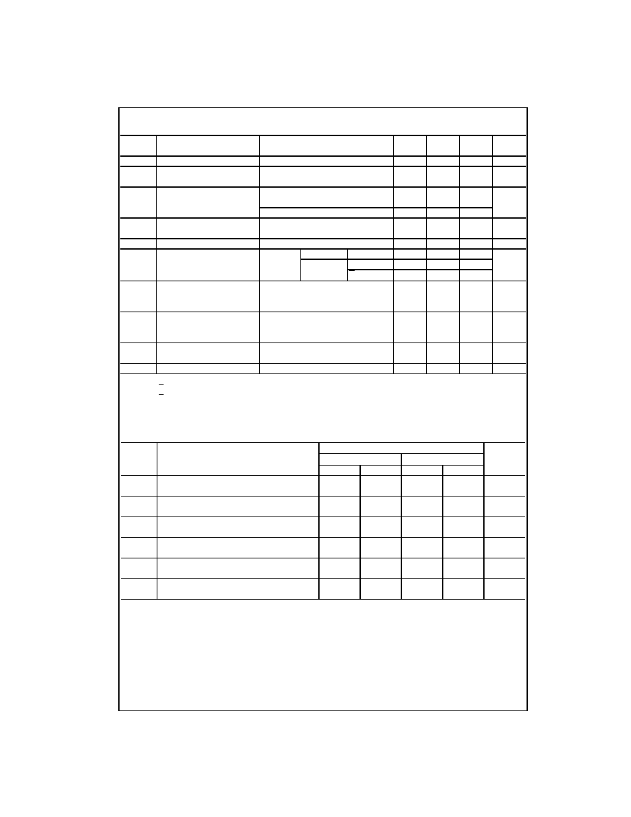
DC Electrical Characteristics
DM81LS95A and DM81LS97A
over recommended operating free air temperature range (unless otherwise noted)
Note 3: All typicals are at V
CC
=
5V, T
A
=
25
∞
C.
Note 4: Both G inputs are at 2V.
Note 5: Both G inputs are at 0.4V.
Note 6: Not more than one output should be shorted at a time, and the duration should not exceed one second.
AC Electrical Characteristics
DM81LS95A and DM81LS97A
V
CC
=
5V, T
A
=
25
∞
C
Note 7: C
L
=
5 pF.
Symbol
Parameter
Conditions Min
Typ
Max
Units
(Note 3)
V
I
Input Clamp Voltage
V
CC
=
Min, I
I
=
-
18 mA
-
1.5
V
V
OH
HIGH Level Output Voltage
V
CC
=
Min, I
OH
=
Max
2.7
V
V
IL
=
Max, V
IH
=
Min
V
OL
LOW Level Output Voltage
V
CC
=
Min, I
OL
=
Max
0.5
V
I
OL
=
Max, V
IH
=
Min
I
OL
=
12 mA, V
CC
=
Min
0.4
I
I
Input Current @ Max
V
CC
=
Max, V
I
=
7V
0.1
mA
Input Voltage
I
IH
HIGH Level Input Current
V
CC
=
Max, V
I
=
2.7V
20
µ
A
I
IL
LOW Level Input Current
V
CC
=
Max
V
I
=
0.5V
A (Note 4)
-
20
µ
A
V
I
=
0.4V
A (Note 5)
-
50
G
-
50
I
OZH
Off-State Output Current
V
CC
=
Max, V
O
=
2.4V
20
µ
A
with HIGH Level Output
V
IH
=
Min, V
IL
=
Max
Voltage Applied
I
OZL
Off-State Output Current
V
CC
=
Max, V
O
=
0.4V
-
20
µ
A
with LOW Level Output
V
IH
=
Min, V
IL
=
Max
Voltage Applied
I
OS
Short Circuit
V
CC
=
Max
-
20
-
100
mA
Output Current
(Note 6)
I
CC
Supply Current
V
CC
=
Max (Note 4)
16
26
mA
Symbol
Parameter
R
L
=
667
Units
C
L
=
50 pF
C
L
=
150 pF
Min
Max
Min
Max
t
PLH
Propagation Delay Time
16
25
ns
LOW-to-HIGH Level Output
t
PHL
Propagation Delay Time
28
40
ns
HIGH-to-LOW Level Output
t
PZH
Output Enable Time
25
30
ns
to HIGH Level Output
t
PZL
Output Enable Time
30
42
ns
to LOW Level Output
t
PHZ
Output Disable Time
20
ns
from HIGH Level Output (Note 7)
t
PLZ
Output Disable Time
27
ns
from LOW Level Output (Note 7)

5
www.fairchildsemi.com
DM81LS95A
∑ DM81LS96A
∑ DM81LS97A
DC Electrical Characteristics
DM81LS96A
over recommended operating free air temperature range (unless otherwise noted)
Note 8: All typicals are at V
CC
=
5V, T
A
=
25
∞
C.
Note 9: Both G inputs are at 2V.
Note 10: Both G inputs are at 0.4V.
Note 11: Not more than one output should be shorted at a time, and the duration should not exceed one second.
AC Electrical Characteristics
DM81LS96A
V
CC
=
5V, T
A
=
25
∞
C
Note 12: C
L
=
5 pF.
Symbol
Parameter
Conditions Min
Typ
Max
Units
(Note 8)
V
I
Input Clamp Voltage
V
CC
=
Min, I
I
=
-
18 mA
-
1.5
V
V
OH
HIGH Level Output Voltage
V
CC
=
Min, I
OH
=
Max
2.7
V
V
IL
=
Max, V
IH
=
Min
V
OL
LOW Level Output Voltage
V
CC
=
Min, I
OL
=
Max
0.5
V
I
OL
=
Max, V
IH
=
Min
I
OL
=
12 mA, V
CC
=
Min
0.4
I
I
Input Current @ Max
V
CC
=
Max, V
I
=
7V
0.1
mA
Input Voltage
I
IH
HIGH Level Input Current
V
CC
=
Max, V
I
=
2.7V
20
µ
A
I
IL
LOW Level Input Current
V
CC
=
Max
V
I
=
0.5V
A (Note 9)
-
20
µ
A
V
I
=
0.4V
A (Note 10)
-
50
G
-
50
I
OZH
Off-State Output Current
V
CC
=
Max, V
O
=
2.4V
20
µ
A
with HIGH Level Output
V
IH
=
Min, V
IL
=
Max
Voltage Applied
I
OZL
Off-State Output Current
V
CC
=
Max, V
O
=
0.4V
-
20
µ
A
with LOW Level Output
V
IH
=
Min, V
IL
=
Max
Voltage Applied
I
OS
Short Circuit
V
CC
=
Max
-
20
-
100
mA
Output Current
(Note 11)
I
CC
Supply Current
V
CC
=
Max (Note 10)
13
21
mA
Symbol
Parameter
R
L
=
667
Units
C
L
=
50 pF
C
L
=
150 pF
Min
Max
Min
Max
t
PLH
Propagation Delay Time
10
16
ns
LOW-to-HIGH Level Output
t
PHL
Propagation Delay Time
17
30
ns
HIGH-to-LOW Level Output
t
PZH
Output Enable Time
15
30
ns
to HIGH Level Output
t
PZL
Output Enable Time
35
45
ns
to LOW Level Output
t
PHZ
Output Disable Time
20
ns
from HIGH Level Output (Note 12)
t
PLZ
Output Disable Time
27
ns
from LOW Level Output (Note 12)
