 | –≠–ª–µ–∫—Ç—Ä–æ–Ω–Ω—ã–π –∫–æ–º–ø–æ–Ω–µ–Ω—Ç: FAN1654 | –°–∫–∞—á–∞—Ç—å:  PDF PDF  ZIP ZIP |

www.fairchildsemi.com
REV. 1.0.5 4/17/02
Features
∑ Sinks and sources 1A continuous, 1.5A peak
∑ -40∞C to +125∞C Operating Range
∑ Load regulation: (VDDQ/2) ± 40mV
∑ 5mA VREF buffer tracks VTT
∑ On-chip thermal limiting
∑ Power-enhanced eTSSOPTM-16 package
∑ Low Current Shutdown Mode
∑ Output Short Circuit Protection
Applications
∑ DDR terminators
Description
The FAN1654 is a low-cost bi-directional LDO specifically
designed for terminating DDR memory bus. It can both sink
and source up to 1A continuous, 1.5A peak, providing
enough current for most DDR applications. Load regulation
meets the JEDEC spec, VTT = (VDDQ/2) ± 40mV.
The FAN1654 includes a buffered reference voltage capable
of supplying up to 5mA current. On-chip thermal limiting
provides protection against a combination of power overload
and ambient temperature that would create an excessive
junction temperature. A shutdown input puts the FAN1654
into a low power mode for laptop computer applications.
The FAN1654 regulator is available in a power-enhanced
eTSSOPTM-16 package, and the standard SOIC-14
Block Diagram
VSS
VSS
VSS
+
-
VTTSENSE
VTTFORCE
VTTFORCE
+
-
VDD
VDD
VDD
SHDN
VDDQ
200k
200k
FAN1655
VSSQ
VREFIN
VREFOUT
FAN1654
1.5A LDO, DDR Bus Termination Regulator

PRODUCT SPECIFICATION
FAN1654
2
REV. 1.0.5 4/17/02
Pin Assignments
Pin Definitions
* Pin Numbers in brackets are for the SOIC-14 package
Typical Application
Pin Number*
Pin Name
Pin Function Description
1, 2, 7 (4, 5, 10)
VDD
VDD.
Input power for the LDO.
3, 6 (6, 9)
VTTFORCE
VTT Force Output.
4, 5, 8 (7, 8, 11)
VSS
Power Ground.
10 (12)
VTTSENSE
VTT Sense
. Feedback for remote sense of the VTT voltage.
11 (13)
VREFIN
VREFIN
. Alternative input for direct control of VTTOUT and VREFOUT.
12 (14)
SHDN
Shutdown.
This active low shutdown turns off both VTT and VREFOUT. This
pin has an internal pull-down, and must be externally driven high for the IC to be
on.
13 (1)
VSSQ
Signal Ground.
14 (2)
VREFOUT
Buffered Voltage Reference Output.
15 (3)
VDDQ
VDDQ Input.
Attach this pin to the VDDQ supply to generate VTT and
VREFOUT.
9,16
NC
No Internal Connection
14
13
12
11
10
9
8
1
2
3
4
5
6
7
FAN1654
SHDN
VREFIN
VTTSENSE
VSS
VDD
VTTFORCE
VSS
VSSQ
VREFOUT
VDDQ
VDD
VDD
VTTFORCE
VSS
16
15
14
13
12
11
10
9
1
2
3
4
5
6
7
8
FAN1654
NC
VDDQ
VREFOUT
VSSQ
SHDN
VREFIN
VTTSENSE
NC
VDD
VDD
VTTFORCE
VSS
VSS
VTTFORCE
VDD
VSS
16-Lead Plastic eTSSOP-16
JC
= 4∞C/W*
*With package power slug soldered to 0.5 square inch
copper area over backside ground plane of internal
power plane
14-Lead Plastic SOIC
JC
= 37∞C/W,
JA
= 88∞C/W
16
15
14
13
12
11
10
9
1
2
3
4
5
6
7
8
100
µF
6V
10
µF
GND
VDD
1nF
(connect to VTTFORCE
at the load)
VTTSENSE
470
µF
10
µF
VTTFORCE
1nF
GND
VREFOUT
SHDN
VDDQ
10k
FAN1654
Figure 1. (eTSSOP pinout shown)

FAN1654
PRODUCT SPECIFICATION
REV. 1.0.5 4/17/02
3
-40
-20
0
20
40
60
80
Quiescent Current vs. Temperature
QUIESCENT CURRENT (mA)
AMBIENT TEMPERATURE
(∞C)
2
1.5
0
.5
1
-60
100
120
140
2.5
3
3.5
-5
-4
-3
-2
-1
0
1
V
REF
Output Change vs. I
REF
V
REFOUT
(mV)
V
REF
LOAD CURRENT (mA)
0.5
0
-1.0
-0.5
-6
2
3
4
1.0
5
6
R
OUT
= 0.2
V
DD
= V
DDQ
= 2.5V
T
A
= 25∞C
1.240
1.245
1.250
1.255
1.260
V
DD
= V
DDQ
= 2.5V
T
A
= 25∞C
V
TT
Load Current
-1500
-1000
-500
0
500
1000
1500
V
TT
Load Current (mA)
V
TT
OUTPUT (V)
Figure 2
Figure 3
Figure 4
Typical Performance Characteristics
PRODUCT SPECIFICATION
FAN1654
4
REV. 1.0.5 4/17/02
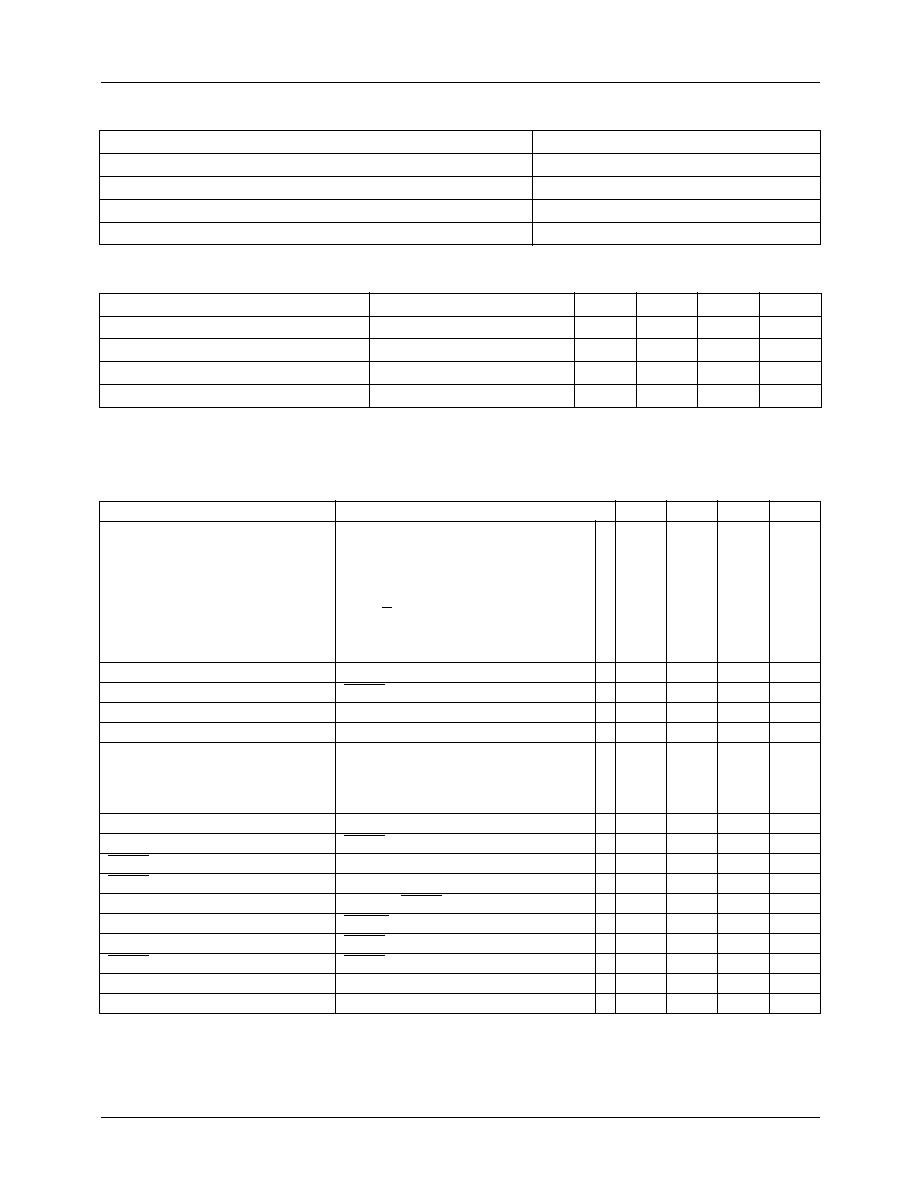
Absolute Maximum Ratings
Recommended Operating Conditions
Electrical Characteristics
(VDD = VDDQ = 2.5V ± 0.2V, and T
A
= 25∞C using circuit in Figure 1, unless otherwise noted.)
The ∑ denotes specifications which apply over the specified operating temperature range.
Supply Voltage VDD, VDDQ
6V
Junction Temperature, T
J
150∞C
Storage Temperature
-65 to 150∞C
Lead Soldering Temperature, 10 seconds
300∞C
Power Dissipation, P
D
1.4W
Parameter
Conditions
Min.
Typ.
Max.
Units
Supply Voltage VDD
2.3
2.5
3.6
V
Supply Voltage VDDQ
2.2
2.5
3.0
V
Ambient Operating Temperature
-40
125
∞C
VREFIN
1.1
1.25
1.5
V
Parameter
Conditions
Min.
Typ.
Max.
Units
VTT Output Voltage
I
OUT
= 0A, VREFIN = open
VDDQ = 2.3V
VDDQ = 2.5V
VDDQ = 2.7V
I
OUT
= +1A, VREFIN = open
VDDQ = 2.3V
VDDQ = 2.5V
VDDQ = 2.7V
∑
∑
∑
1.135
1.235
1.335
1.110
1.210
1.310
1.150
1.250
1.350
1.150
1.250
1.350
1.165
1.265
1.365
1.190
1.290
1.390
V
V
V
V
V
V
VTT Output Slew Rate
Cload = 10µF
0.1
V/µsec
VTT Leakage Current
SHDN = 0V
∑
-50
50
µA
VTT Current Limit
±2
A
VREFIN Input Impedance
100
K
VREFOUT Output Voltage
No load
VREFIN = 1.150V
VREFIN = 1.250V
VREFIN = 1.350V
∑
∑
∑
1.145
1.245
1.345
1.150
1.250
1.350
1.155
1.255
1.355
V
V
V
VREFOUT Output Current
VDDQ = 2.3V
∑
-5
5
mA
VREFOUT Leakage Current
SHDN = 0V
∑
-10
10
µA
SHDN Logic High
∑
1.667
V
SHDN Logic Low
∑
0.800
V
IDD Supply Current
No load, SHDN = 2.7V
∑
3
10
mA
VDDQ Leakage Current
SHDN = 0V
∑
6
10
µA
VDD Leakage Current
SHDN = 0V
∑
3
50
µA
SHDN Input Current
SHDN = 2.7V
∑
50
75
µA
Over-Temperature Shutdown
155
∞C
Over-Temperature Hysteresis
30
∞C

FAN1654
PRODUCT SPECIFICATION
REV. 1.0.5 4/17/02
5
Mechanical Dimensions
16 Lead eTSSOP
6.4
5.0
± 0.1
0.10 TYP
4.4
± 0.1
7.72
4.16
3.40
4.00
(1.78)
0.42 TYP
0.65 TYP
1.7 MIN
1.5 MIN
0.25
SEATING PLANE
SEE DETAIL A
DETAIL A
(1.00)
0.75
0.45
GAGE PLANE
LAND PATTERN RECOMMENDATION
0
∞≠8∞
R0.09MIN
12
∞ TOP & BOTTOM
-A-
-B-
0.65 TYP
0.10
C B A
M
-C-
3.2
(0.90)
+0.15
≠0.10
(0.09≠0.20)
(0.19≠0.30)
0.10
±0.05 TYP
1.2 MAX
PIN #1 IDENT.
NOTES:
A. CONFORMS TO JEDEC REGISTRATION MO-153, VARIATION ABT,
DATED
10/97.
B. DIMENSIONS ARE IN MILLIMETERS.
C. DIMENSIONS ARE EXCLUSIVE OF BURRS, MOLD FLASH,
AND THE BAR EXTENSIONS.
D. DIMENSIONS AND TOLERANCES PER ASME Y14.5M, 1994.
BOTTOM VIEW
0.2
ALL LEAD TIPS
ALL LEAD TIPS
C B A
0.1
1
8
1
1
8
8
9
16
9
9
16
16
C