 | –≠–ª–µ–∫—Ç—Ä–æ–Ω–Ω—ã–π –∫–æ–º–ø–æ–Ω–µ–Ω—Ç: FAN1851AN | –°–∫–∞—á–∞—Ç—å:  PDF PDF  ZIP ZIP |
www.fairchildsemi.com
REV. 2.0.1 6/17/05
Features
∑ Improved performance over industry equivalents
≠ Tight fault current range (Typ ±100µA)
≠ Temperature compensated fault current characteristics
≠ No external trimming required
∑ Direct interface to SCR
∑ Supply voltage derived from AC line--26V shunt
∑ Adjustable sensitivity
∑ Grounded neutral fault detection
∑ Meets UL943 standards
∑ 450µA quiescent current
∑ Ideal for 120V or 220V systems
∑ Package options: 8L DIP and 8L SOIC
Description
The FAN1851A is a controller for AC outlet ground fault
interrupters. These devices detect hazardous grounding con-
ditions (example: a pool of water or an electrical equipment
connected to opposite phases of the AC line) in consumer
and industrial environments. The output of the IC triggers an
external SCR, which in turn opens a relay circuit breaker to
prevent a harmful or lethal shock.
Full advantage of the U.S. UL943 timing specification is
taken to ensure maximum immunity to false triggering due
to line noise. A special feature in the circuitry rapidly resets
the integrating timing capacitor in the event that noise pulses
introduce unwanted charging currents. Also, a flip-flop is
included that ensures firing of even a slow circuit breaker
relay on either of the two half-cycles of the line voltage
when external full wave rectification is used.
The application circuit can be configured to detect both
normal faults (hot wire to ground) and grounded neutral
faults.
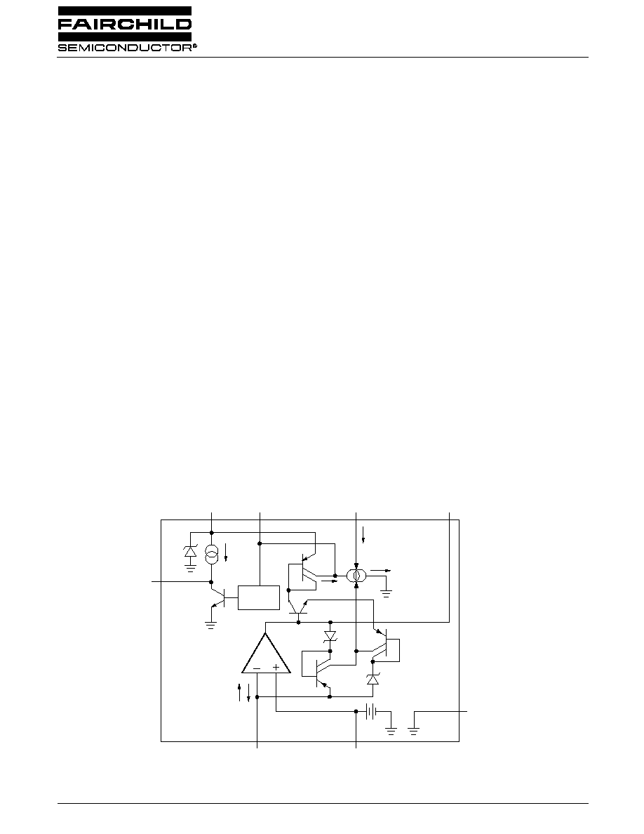
Block Diagram
+V
S
Timing
Capacitor
Sensitivity
Set Resistor
I
TH
Sense Amplifier
Output
I
TH
for I
F
> 0
3I
TH
for I
F
= 0
I
1
=
I
F
Q2
Q1
Latch
D3
I
2
Q3
Q4
A1
D1
I
F
Ground
Non-Inverting Input
10V
Inverting Input
SCR Trigger
Q5
D2
+V
S
FAN1851A
Ground Fault Interrupter

FAN1851A
PRODUCT SPECIFICATION
2
REV. 2.0.1 6/17/05
Functional Description
The voltage at the supply pin is clamped to +26V by the
internal shunt regulator D3. This shunt regulator also
generates an artificial ground voltage for the noninverting
input of A1 (shown as a +10V source). A1, Q1, and Q2
together act as a current mirror for fault current signals
(which are derived from an external transformer). When a
fault signal is present, the mirrored current charges the
external timing capacitor until its voltage exceeds the latch
trigger threshold (typically 17.5V). When this threshold is
exceeded, the latch engages and Q3 turns off, allowing I
2
to
drive the SCR connected to the "SCR Trigger" pin.
Extra Circuitry in the feedback path of A1 works with the
switched current source I
1
to remove any charge on C
T
induced by noise in the transformer. If no fault current is
present, then I
1
discharges C
T
with a current equal to 3 I
TH
,
where I
TH
is the value of current set by the external R
SET
resistor. If fault signals are present at the input of A1 (which
is held at virtual ground, +10V), one of the two current
mirrors in the feedback path of A1 (Q4 and Q5) will become
active, depending on which half-cycle the fault occurs.
This action will raise the voltage at V
S
, switching I
1
to a
value equal to I
TH
, and reducing the discharge rate of C
T
to
better allow fault currents to charge it.
Notice that I
TH
discharges C
T
during both half-cycles of the
line, while I
F
only charges C
T
during the half-cycle in which
I
F
exits the "- Input" pin (since Q1 will only carry fault cur-
rent in one direction). Thus, during one half-cycle, I
F
-I
TH
charges C
T
, while during the other half-cycle I
TH
discharges
it.
Pin Assignments
SCR Trigger
≠ Input
+ Input
Ground
+V
S
C
T
R
SET
Amp Out
1
2
3
4
8
7
6
5
Definition of Terms
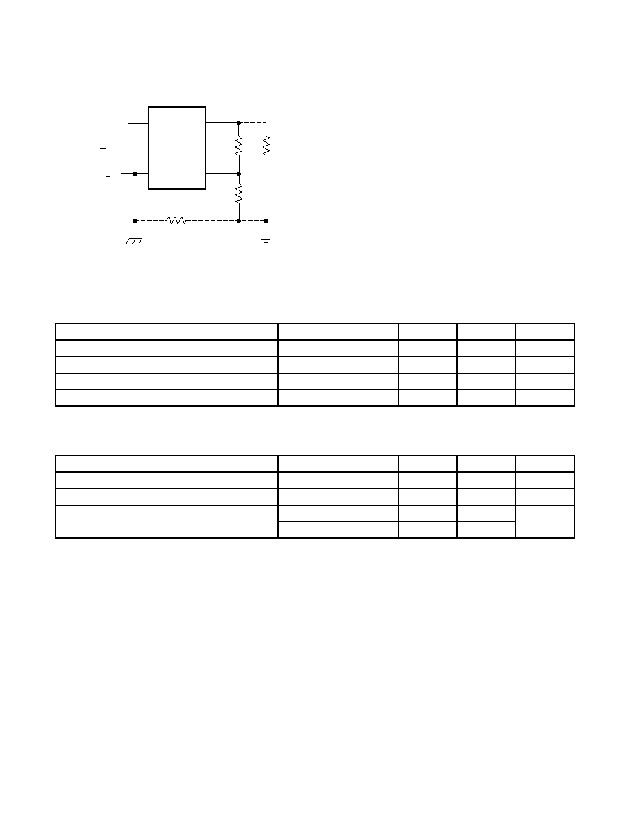
Normal Fault:
An unintentional electrical path, R
B
, between the load termi-
nal of the hot line and the ground, as shown by the dashed
lines in Figure1.
Figure 1. Normal Fault
Grounded Neutral Fault:
An unintentional electrical path between the load terminal of
the neutral line and the ground, as shown by the dashed lines
in Figure 2.
Figure 2. Grounded Neutral Fault
Hot
GFI
Neutral
Line
Hot
R
LOAD
R
B
Neutral
R
G
Hot
GFI
Neutral
Line
Hot
R
LOAD
R
IN
Neutral
R
G
PRODUCT SPECIFICATION
FAN1851A
REV. 2.0.1 6/17/05
3
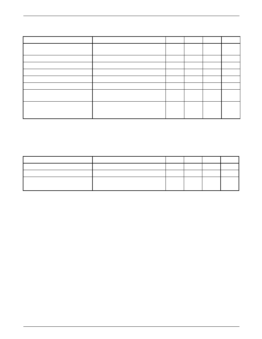
Normal Fault Plus Grounded Neutral Fault:
The combination of the normal fault and the grounded
neutral fault, as shown by the dashed lines in Figure 3.
Figure 3. Normal Fault Plus Grounded Neutral Fault
Absolute Maximum Ratings
Thermal Characteristics
Parameter
Conditions
Min
Max
Units
Supply Current
19
mA
Power Dissipation
570
mW
Operating Temperature
-40
70
∞C
Lead Soldering Temperature, 60 seconds
300
∞C
Parameter
Conditions
Min
Max
Units
Maximum Junction Temperature
125
∞C
Maximum P
D
T
A
< 50∞C
468
mW
Thermal Resistance,
JA
DIP
85
∞C/W
SOIC
150
Hot
GFI
Neutral
Line
Hot
R
LOAD
R
B
Neutral
R
G
R
N
FAN1851A
PRODUCT SPECIFICATION
4
REV. 2.0.1 6/17/05
DC Electrical Characteristics
(T
A
= +25∞C, I
SHUNT
= 5 mA)
Note:
1. This external applied current is in addition to the internal "output drive current" source.
AC Electrical Characteristics
(T
A
= +25∞C, I
SHUNT
= 5 mA)
Notes:
1. Average of ten trials.
2. Required UL System sensitivity tolerance is 4mA to 6mA.
Parameters
Test Conditions
Min
Typ
Max
Units
Power Supply Shunt Regulator
Voltage
Pin 8, Average Value
22
26
30
V
Latch Trigger Voltage
Pin 7
15
17.5
20
V
Sensitivity Set Voltage
Pin 8 to Pin 6
6
7
8.2
V
Output Drive Current
Pin 1 With Fault
0.5
1
2.4
mA
Output Saturation Voltage
Pin 1 Without Fault
100
240
mV
Output Saturation Resistance
Pin 1 Without Fault
100
Output External Current Sinking
Capability
1
Pin 1 Without Fault, V
PIN1
Held
to 0.3V
2
5
mA
Noise Integration Sink Current
Ratio
Pin 7, Ratio of Discharge Currents
Between No Fault and Fault
Conditions
2.0
2.8
3.6
µA/µA
Parameters
Conditions
Min
Typ
Max
Units
Normal Fault Current Sensitivity
2
See Figure 9
4.75
5
5.25
mA
Normal Fault Trip Time
1
500
Fault, see Figure 10
18
mS
Normal Fault With Grounded
500
Normal Fault,
18
mS
Neutral Fault Trip Time
1
2
Neutral, see Figure 10 (Note 1)

PRODUCT SPECIFICATION
FAN1851A
REV. 2.0.1 6/17/05
5
Typical Performance Characteristics
(T
A
= +25∞C)
Figure 4. Average Trip Time vs. Fault Current
Figure 5. Normal Fault Current Threshold vs. R
SET
Figure 6. Output Drive Current vs. Output Voltage
Figure 7. Pin 1 Saturation Voltage vs.
External Load Current, I
L
0.01
0.1
1
1000
100
10
0
Trip Time (Seconds)
Fault Current (mA)
Circuit of
Figure 10
UL943
Normal
Fault
10
100K
1M
10M
100
10
1
R
SET
(
)
Fault Current on Line [mA(rms)]
7V
I
F
(rms)* x (0.91)
Sense Transformer 1000:1
R
SET
=
1400
1200
1000
800
600
400
200
0
Output Voltage @ V
PIN1
(V)
Output Drive Current @ Pin 1 (
A)
35
30
25
20
15
10
5
0
A
5 mA
31V
1 mA
8
1
4
V
PIN1
0.1
1
10
100
10
1
0.1
0.01
External Load Current (mA)
Pin 1 Saturation Voltage (V)
V
5 mA
31V
I
L
1 mA
8
1
4