
www.fairchildsemi.com
REV. 1.2.3 11/2/04
Features
∑ Internally synchronized PFC and PWM in one 8-pin IC
∑ Patented one-pin voltage error amplifier with advanced
input current shaping technique
∑ Peak or average current, continuous boost, leading edge
PFC (Input Current Shaping Technology)
∑ High efficiency trailing-edge current mode PWM
∑ Low supply currents; start-up: 150µA typ., operating:
2mA typ.
∑ Synchronized leading and trailing edge modulation
∑ Reduces ripple current in the storage capacitor between
the PFC and PWM sections
∑ Overvoltage, UVLO, and brownout protection
∑ PFC V
CC
OVP with PFC Soft Start
General Description
The FAN4803 is a space-saving controller for power factor
corrected, switched mode power supplies that offers very
low start-up and operating currents.
Power Factor Correction (PFC) offers the use of smaller, lower
cost bulk capacitors, reduces power line loading and stress on
the switching FETs, and results in a power supply fully compli-
ant to IEC1000-3-2 specifications. The FAN4803 includes
circuits for the implementation of a leading edge, average
current "boost" type PFC and a trailing edge, PWM.
The FAN4803-1's PFC and PWM operate at the same
frequency, 67kHz. The PFC frequency of the FAN4803-2 is
automatically set at half that of the 134kHz PWM. This
higher frequency allows the user to design with smaller
PWM components while maintaining the optimum operating
frequency for the PFC. An overvoltage comparator shuts
down the PFC section in the event of a sudden decrease in
load. The PFC section also includes peak current limiting for
enhanced system reliability.
Block Diagram
ISENSE
3
VEAO
4
VDC
5
ILIMIT
6
GND
2
PWM OUT
8
PFC OUT
1
≠
+
≠
+
COMP
COMP
35
µ
A
16.2V
17.5V
VCC
+
≠
COMP
+
≠
≠1V
SOFT START
PFC/PWM UVLO
DUTY CYCLE
LIMIT
OSCILLATOR
PFC ≠ 67kHz
PWM ≠ 134kHz
VREF
VREF
1.2V
26k
40k
M1
R1
C1
30pF
M2
M7
M3
M4
M6
PWM
CONTROL
LOGIC
≠
+
1.5V
DC ILIMIT
PFC ILIMIT
PWM COMPARATOR
VCC OVP
PFC OFF
ONE PIN ERROR AMPLIFIER
LEADING
EDGE PFC
TRAILING
EDGE PWM
+
≠
COMP
7V
+
≠
COMP
≠1
≠4
REF
VCC
7
PFC
CONTROL
LOGIC
FAN4803
8-Pin PFC and PWM Controller Combo
FAN4803
PRODUCT SPECIFICATION
2
REV. 1.2.3 11/2/04
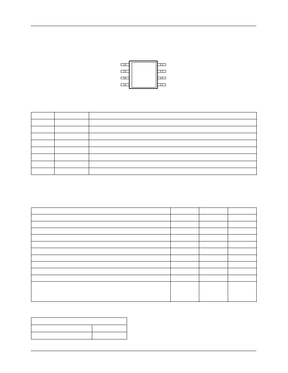
Pin Configuration
Pin Description
1
2
3
4
8
7
6
5
PFC OUT
GND
ISENSE
VEAO
PWM OUT
VCC
ILIMIT
VDC
TOP VIEW
8-Pin SOIC (S08)
8-Pin PDIP (P08)
FAN4803
Pin Name
Function
1
PFC OUT
PFC driver output
2
GND
Ground
3
I
SENSE
Current sense input to the PFC current limit comparator
4
VEAO
PFC one-pin error amplifier input
5
V
DC
PWM voltage feedback input
6
I
LIMIT
PWM current limit comparator input
7
V
CC
Positive supply (may require an external shunt regulator)
8
PWM OUT
PWM driver output
Absolute Maximum Ratings
Absolute maximum ratings are those values beyond which the device could be permanently damaged. Absolute maximum
ratings are stress ratings only and functional device operation is not implied.
Operating Conditions
Parameter
Min
Max
Unit
I
CC
Current (average)
40
mA
V
CC
MAX
18.3
V
I
SENSE
Voltage
-5
1
V
Voltage on Any Other Pin
GND ≠ 0.3
V
CC
+ 0.3
V
Peak PFC OUT Current, Source or Sink
1
A
Peak PWM OUT Current, Source or Sink
1
A
PFC OUT, PWM OUT Energy Per Cycle
1.5
µJ
Junction Temperature
150
∞C
Storage Temperature Range
-65∞
150
∞C
Lead Temperature (Soldering, 10 sec)
260
∞C
Thermal Resistance (
JA
)
Plastic DIP
110
∞C/W
Plastic SOIC
160
∞C/W
Temperature Range
FAN4803CS-X
0∞C to 70∞C
FAN4803CP-X
0∞C to 70∞C

PRODUCT SPECIFICATION
FAN4803
REV. 1.2.3 11/2/04
3
Electrical Characteristics
Unless otherwise specified, V
CC
= 15V, T
A
= Operating Temperature Range (Note 1)
Note:
1. Limits are guaranteed by 100% testing, sampling, or correlation with worst case test conditions.
Symbol
Parameter
Conditions
Min
TYP
MAX UNITS
One-pin Error Amplifier
V
EAO
Output Current
T
A
= 25∞C, V
EAO
= 6V
34.0
36.5
39.0
µA
Line Regulation
10V < V
CC
< 15V, V
EAO
= 6V
0.1
0.3
µA
V
CC
OVP Comparator
Threshold Voltage
15.5
16.3
16.8
V
PFC I
LIMIT
Comparator
Threshold Voltage
-0.9
-1
-1.15
V
Delay to Output
150
300
ns
DC I
LIMIT
Comparator
Threshold Voltage
1.4
1.5
1.6
V
Delay to Output
150
300
ns
Oscillator
Initial Accuracy
T
A
= 25∞C
60
67
74
kHz
Voltage Stability
10V < V
CC
< 15V
1
%
Temperature Stability
2
%
Total Variation
Over Line and Temp
60
67
74.5
kHz
Dead Time
PFC Only
0.3
0.45
0.65
µs
PFC
Minimum Duty Cycle
V
EAO
> 7.0V,I
SENSE
= -0.2V
0
%
Maximum Duty Cycle
V
EAO
< 4.0V,I
SENSE
= 0V
90
95
%
Output Low Impedance
8
15
Output Low Voltage
I
OUT
= ≠100mA
0.8
1.5
V
I
OUT
= ≠10mA, V
CC
= 8V
0.7
1.5
V
Output High Impedance
8
15
Output High Voltage
I
OUT
= 100mA, V
CC
= 15V
13.5
14.2
V
Rise/Fall Time
C
L
= 1000pF
50
ns
PWM
Duty Cycle Range
FAN4803-2
0-41
0-47
0-50
%
FAN4803-1
0-49.5
0-50
%
Output Low Impedance
8
15
Output Low Voltage
I
OUT
= ≠100mA
0.8
1.5
V
I
OUT
= ≠10mA, V
CC
= 8V
0.7
1.5
V
Output High Impedance
8
15
Output High Voltage
I
OUT
= 100mA, V
CC
= 15V
13.5
14.2
V
Rise/Fall Time
C
L
= 1000pF
50
ns
Supply
V
CC
Clamp Voltage (V
CCZ
)
I
CC
= 10mA
16.7
17.5
18.3
V
Start-up Current
V
CC
= 11V, C
L
= 0
0.2
0.4
mA
Operating Current
V
CC
= 15V, C
L
= 0
2.5
4
mA
Undervoltage Lockout Threshold
11.5
12
12.5
V
Undervoltage Lockout Hysteresis
2.4
2.9
3.4
V
FAN4803
PRODUCT SPECIFICATION
4
REV. 1.2.3 11/2/04
Functional Description
The FAN4803 consists of an average current mode boost
Power Factor Corrector (PFC) front end followed by a syn-
chronized Pulse Width Modulation (PWM) controller. It is
distinguished from earlier combo controllers by its low pin
count, innovative input current shaping technique, and very
low start-up and operating currents. The PWM section is
dedicated to peak current mode operation. It uses conven-
tional trailing-edge modulation, while the PFC uses leading-
edge modulation. This patented Leading Edge/Trailing Edge
(LETE) modulation technique helps to minimize ripple cur-
rent in the PFC DC buss capacitor.
The FAN4803 is offered in two versions. The FAN4803-1
operates both PFC and PWM sections at 67kHz, while the
FAN4803-2 operates the PWM section at twice the fre-
quency (134kHz) of the PFC. This allows the use of smaller
PWM magnetics and output filter components, while mini-
mizing switching losses in the PFC stage.
In addition to power factor correction, several protection fea-
tures have been built into the FAN4803. These include soft
start, redundant PFC over-voltage protection, peak current
limiting, duty cycle limit, and under voltage lockout
(UVLO). See Figure 12 for a typical application.
Detailed Pin Descriptions
V
EAO
This pin provides the feedback path which forces the PFC
output to regulate at the programmed value. It connects to
programming resistors tied to the PFC output voltage and is
shunted by the feedback compensation network.
I
SENSE
This pin ties to a resistor or current sense transformer which
senses the PFC input current. This signal should be negative
with respect to the IC ground. It internally feeds the pulse-
by-pulse current limit comparator and the current sense feed-
back signal. The I
LIMIT
trip level is ≠1V. The I
SENSE
feed-
back is internally multiplied by a gain of four and compared
against the internal programmed ramp to set the PFC duty
cycle. The intersection of the boost inductor current
downslope with the internal programming ramp determines
the boost off-time.
V
DC
This pin is typically tied to the feedback opto-collector. It is
tied to the internal 5V reference through a 26k
resistor and
to GND through a 40k
resistor.
I
LIMIT
This pin is tied to the primary side PWM current sense resis-
tor or transformer. It provides the internal pulse-by-pulse
current limit for the PWM stage (which occurs at 1.5V) and
the peak current mode feedback path for the current mode
control of the PWM stage. The current ramp is offset inter-
nally by 1.2V and then compared against the opto feedback
voltage to set the PWM duty cycle.
PFC OUT and PWM OUT
PFC OUT and PWM OUT are the high-current power driv-
ers capable of directly driving the gate of a power MOSFET
with peak currents up to ±1A. Both outputs are actively held
low when V
CC
is below the UVLO threshold level.
V
CC
V
CC
is the power input connection to the IC. The V
CC
start-
up current is 150µA . The no-load I
CC
current is 2mA. V
CC
quiescent current will include both the IC biasing currents
and the PFC and PWM output currents. Given the operating
frequency and the MOSFET gate charge (Qg), average
PFC and PWM output currents can be calculated as I
OUT
=
Qg x F. The average magnetizing current required for any
gate drive transformers must also be included. The V
CC
pin
is also assumed to be proportional to the PFC output voltage.
Internally it is tied to the V
CC
OVP comparator (16.2V)
providing redundant high-speed over-voltage protection
(OVP) of the PFC stage. V
CC
also ties internally to the
UVLO circuitry, enabling the IC at 12V and disabling it at
9.1V. V
CC
must be bypassed with a high quality ceramic
bypass capacitor placed as close as possible to the IC.
Good bypassing is critical to the proper operation of the
FAN4803.
V
CC
is typically produced by an additional winding off the
boost inductor or PFC Choke, providing a voltage that is pro-
portional to the PFC output voltage. Since the V
CC
OVP max
voltage is 16.2V, an internal shunt limits V
CC
overvoltage to
an acceptable value. An external clamp, such as shown in
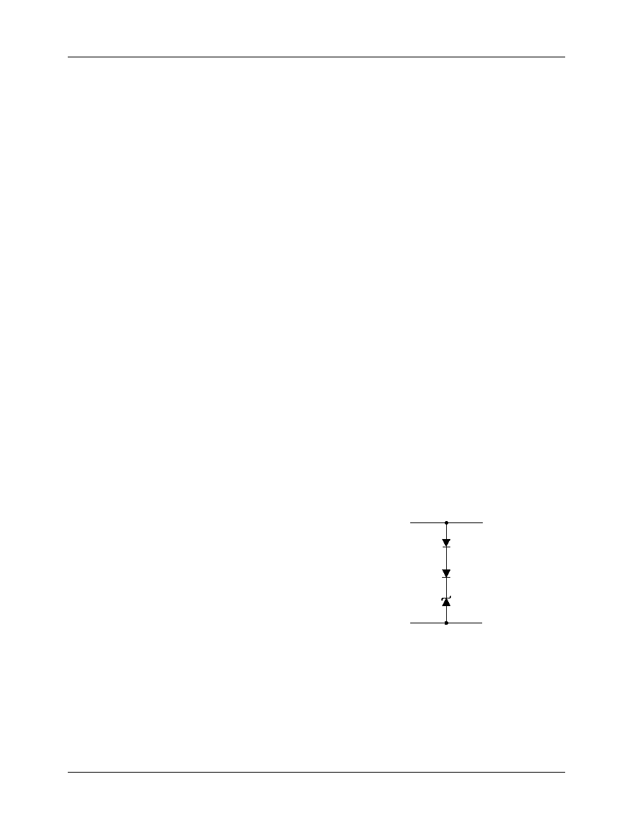
Figure 1, is desirable but not necessary.
Figure 1. Optional V
CC
Clamp
V
CC
is internally clamped to 16.7V minimum, 18.3V maxi-
mum. This limits the maximum V
CC
that can be applied to
the IC while allowing a V
CC
which is high enough to trip the
V
CC
OVP. The max current through this zener is 10mA.
External series resistance is required in order to limit the
current through this Zener in the case where the V
CC
voltage
exceeds the zener clamp level.
VCC
GND
1N4148
1N4148
1N5246B

PRODUCT SPECIFICATION
FAN4803
REV. 1.2.3 11/2/04
5
GND
GND is the return point for all circuits associated with
this part. Note: a high-quality, low impedance ground is
critical to the proper operation of the IC. High frequency
grounding techniques should be used.
Power Factor Correction
Power factor correction makes a nonlinear load look like a
resistive load to the AC line. For a resistor, the current drawn
from the line is in phase with, and proportional to, the line
voltage. This is defined as a unity power factor is (one). A
common class of nonlinear load is the input of a most power
supplies, which use a bridge rectifier and capacitive input fil-
ter fed from the line. Peak-charging effect, which occurs on
the input filter capacitor in such a supply, causes brief high-
amplitude pulses of current to flow from the power line,
rather than a sinusoidal current in phase with the line volt-
age. Such a supply presents a power factor to the line of less
than one (another way to state this is that it causes significant
current harmonics to appear at its input). If the input current
drawn by such a supply (or any other nonlinear load) can be
made to follow the input voltage in instantaneous amplitude,
it will appear resistive to the AC line and a unity power factor
will be achieved.
To hold the input current draw of a device drawing power
from the AC line in phase with, and proportional to, the input
voltage, a way must be found to prevent that device from
loading the line except in proportion to the instantaneous line
voltage. The PFC section of the FAN4803 uses a boost-
mode DC-DC converter to accomplish this. The input to the
converter is the full wave rectified AC line voltage. No filter-
ing is applied following the bridge rectifier, so the input
voltage to the boost converter ranges, at twice line frequency,
from zero volts to the peak value of the AC input and back to
zero. By forcing the boost converter to meet two simulta-
neous conditions, it is possible to ensure that the current that
the converter draws from the power line matches the instan-
taneous line voltage. One of these conditions is that the
output voltage of the boost converter must be set higher than
the peak value of the line voltage. A commonly used value is
385VDC, to allow for a high line of 270VAC
RMS
. The other
condition is that the current that the converter is allowed to
draw from the line at any given instant must be proportional
to the line voltage.
Since the boost converter topology in the FAN4803 PFC is
of the current-averaging type, no slope compensation is
required.
Leading/Trailing Modulation
Conventional Pulse Width Modulation (PWM) techniques
employ trailing edge modulation in which the switch will
turn ON right after the trailing edge of the system clock.
The error amplifier output voltage is then compared with the
modulating ramp. When the modulating ramp reaches the
level of the error amplifier output voltage, the switch will be
turned OFF. When the switch is ON, the inductor current will
ramp up. The effective duty cycle of the trailing edge modu-
lation is determined during the ON time of the switch. Figure
2 shows a typical trailing edge control scheme.
Figure 2. Typical Trailing Edge Control Scheme.
RAMP
VEAO
TIME
VSW1
TIME
REF
EA
≠
+
≠
+
OSC
DFF
R
D
Q
Q
CLK
U1
RAMP
CLK
U4
U3
C1
RL
I4
SW2
SW1
+
DC
I1
I2
I3
VIN
L1
U2