 | –≠–ª–µ–∫—Ç—Ä–æ–Ω–Ω—ã–π –∫–æ–º–ø–æ–Ω–µ–Ω—Ç: FAN5330 | –°–∫–∞—á–∞—Ç—å:  PDF PDF  ZIP ZIP |

©2005 Fairchild Semiconductor Corporation
1
www.fairchildsemi.com
August 2005
FAN5330 Rev. 1.0.1
F
AN5330 High Efficienc
y Serial LED Driver with 30V Integrated Switc
h
FAN5330
High Efficiency Serial LED Driver with 30V Integrated
Switch
Features
1.5MHz Switching Frequency
Low Noise
Adjustable Output Voltage
0.7W Output Power Capability
Low Shutdown Current: <1µA
Cycle-by-Cycle Current Limit
Low Feedback Voltage (110mV)
Over-Voltage Protection
Fixed-Frequency PWM Operation
Internal Compensation
Thermal Shutdown
5-Lead SOT23 Package
Applications
Cell Phones
PDAs
Handheld Equipment
Display Bias
LED Bias
Description
The FAN5330 is an LED driver that features fixed frequency
mode operation and an integrated FET switch. This device is
designed to operate at high switching frequencies in order to
minimize switching noise measured at the battery terminal of
hand-held communications equipment. Quiescent current in
both normal and shutdown mode is designed to be minimal in
order to extend battery life. Normal or shutdown mode can be
selected by a logic level shutdown circuitry.
The low ON-resistance of the internal N-channel switch ensures
high efficiency and low power dissipation. A cycle-by-cycle cur-
rent limit circuit keeps the peak current of the switch below a
typical value of 1.5A. The FAN5330 is available in a 5-lead
SOT23 package.
Typical Application
Figure 1. Typical Application Diagram
SHDN
V
IN
V
OUT
R
GND
V
IN
FB
SW
C
IN
6.8µH to 10µH
1
3
2
4
5
2.2
µF
C
OUT
L
BAT54
I
LED
0.47
µF
ON
OFF
FA
N5330
2
www.fairchildsemi.com
FAN5330 Rev. 1.0.1
F
AN5330 High Efficienc
y Serial LED Driver with 30V Integrated Switc
h
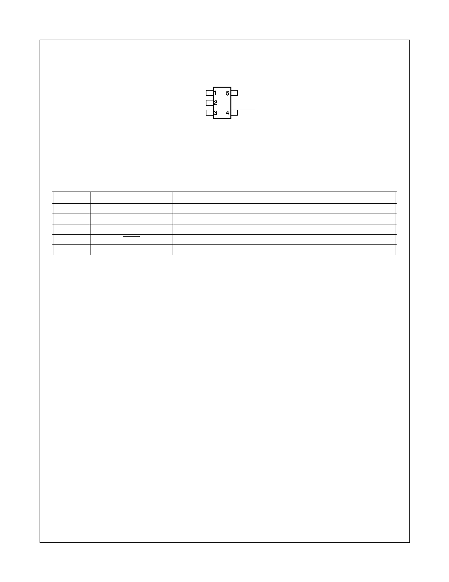
Pin Assignment
Figure 2. Pin Assignment
Pin Description
Pin No.
Pin Name
Pin Description
1
SW
Switching Node.
2
GND
Analog and Power Ground.
3
FB
Feedback Pin.
Feedback node that connects to an external current set resistor.
4
SHDN
Shutdown Control Pin.
Logic HIGH enables, logic LOW disables the device.
5
V
IN
Input Voltage Pin.
SW
GND
FB
V
IN
SHDN
Top View
5-Lead SOT-23
3
www.fairchildsemi.com
FAN5330 Rev. 1.0.1
F
AN5330 High Efficienc
y Serial LED Driver with 30V Integrated Switc
h
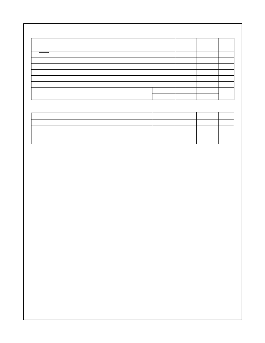
Absolute Maximum Ratings
(
Note1)
Recommended Operating Conditions
Notes:
1.
Stresses above those listed under "Absolute Maximum Ratings" may cause permanent damage to the device. This is a stress
rating only and functional operation of the device at these or any other conditions above those indicated in the operational section
of this specification is not implied. Exposure to absolute maximum rating conditions for extended periods may affect device
reliability. Absolute maximum ratings apply individually only, not in combination.
2.
Using EIA/JESD22A114B (Human Body Model) and EIA/JESD22C101-A (Charge Device Model).
3.
This load capacitance value is required for the loop stability. Tolerance, temperature variation, and voltage dependency of the
capacitance must be considered. Typically a 0.47µF ceramic capacitor is required to achieve specified value at V
OUT
= 30V.
Parameter
Min.
Max.
Unit
V
IN
to GND
6.0
V
FB, SHDN to GND
-0.3
V
IN
+ 0.3
V
SW to GND
-0.3
35
V
Lead Soldering Temperature (10 seconds)
300
∞C
Junction Temperature
150
∞C
Storage Temperature
-55
150
∞C
Thermal Resistance (
JA
)
210
∞C/W
Electrostatic Discharge Protection (ESD) Level (Note 2)
HBM
2
KV
CDM
1
Parameter
Min.
Typ.
Max.
Unit
Input Voltage
1.8
5.5
V
Output Voltage
V
IN
30
V
Operating Ambient Temperature
-40
25
85
∞C
Output Capacitance Rated at the Required Output (Note 3)
0.1
µF
4
www.fairchildsemi.com
FAN5330 Rev. 1.0.1
F
AN5330 High Efficienc
y Serial LED Driver with 30V Integrated Switc
h
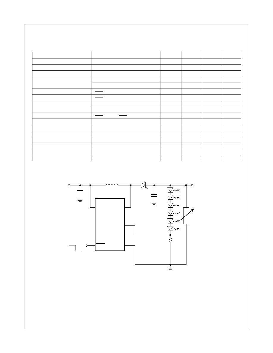
Electrical Characteristics
Test Circuit
Figure 3. Test Circuit
Unless otherwise noted, V
IN
= 3.6V, I
LED
= 20mA, T
A
= -40∞C to 85∞C, Typical values are at T
A
= 25∞C, Test
Circuit, Figure 3.
Parameter
Conditions
Min.
Typ.
Max.
Units
Feedback Voltage
99
110
121
mV
Switch Current Limit
V
IN
= 3.2V
1.1
1.5
A
Load Current Capability
V
OUT
20V V
IN
= 3.2V
35
mA
Switch On-resistance
V
IN
= 5V
0.6
V
IN
= 3.6V
0.7
Quiescent Current
V
SHDN
= 3.6V, No Switching
0.6
mA
OFF Mode Current
V
SHDN
= 0V
0.1
3
µ
A
Shutdown Threshold
Device ON
1.5
V
Device OFF
0.5
V
Shutdown Pin Bias Current
V
SHDN
= 0V or V
SHDN
= 5.5V
1
300
nA
Feedback Pin Bias Current
1
300
nA
Feedback Voltage Line Regulation
2.7V < V
IN
< 5.5V, V
OUT
20V
0.3
%
Switching Frequency
1.25
1.5
1.75
MHz
Maximum Duty Cycle
87
93
%
Switch Leakage Current
No Switching, V
IN
= 5.5V
1
µ
A
OVP
15
%
Thermal Shutdown Temperature
150
∞C
SHDN
V
IN
V
OUT
R
GND
V
IN
FB
SW
C
IN
10
µH
1
3
2
4
5
10
µF
C
OUT
L
BAT54
I
LED
1
µF
ON
OFF
Electronic Load
F
AN5330
5
www.fairchildsemi.com
FAN5330 Rev. 1.0.1
F
AN5330 High Efficienc
y Serial LED Driver with 30V Integrated Switc
h
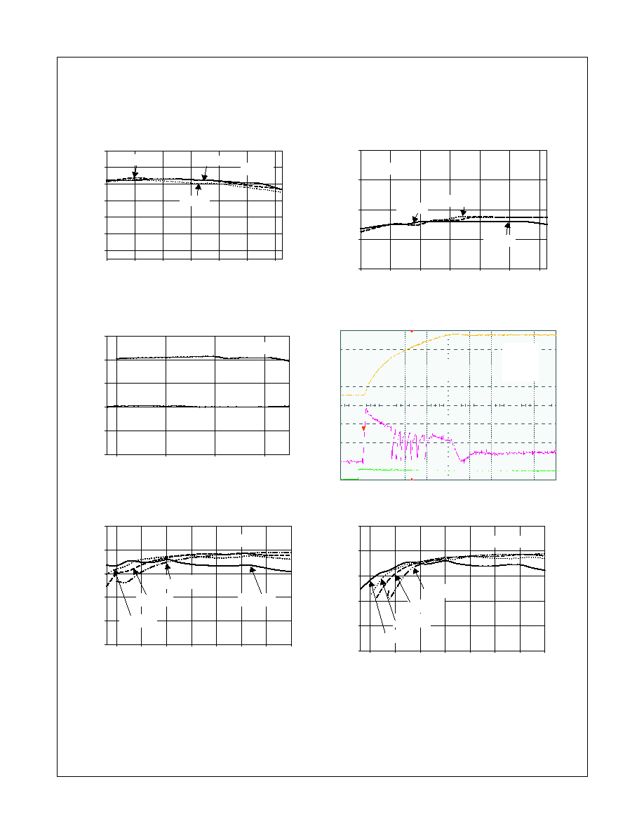
Typical Performance Characteristics
T
A
= 25∞C, C
IN
= 4.7µF, C
OUT
= 0.47µF, L = 10µH, unless otherwise noted.
-40
-20
0
20
40
60
80
9.6
9.8
10.0
10.2
10.4
10.6
10.8
LED Current vs Temperature
LED Current (
mA
)
V
IN
= 2.2V
V
IN
= 3.6V
V
IN
= 5.5V
V
OUT
= 15V
-40
-20
0
20
40
60
80
1.2
1.4
1.6
1.8
2.0
SW Frequency vs. Temperature
Temperature (
∞C)
SW Freq
ue
ncy
(M
Hz)
V
IN
= 2.2V
V
OUT
= 15V
V
IN
= 3.6V
V
IN
= 5.5V
2
3
4
5
0
5
10
15
20
25
V
OUT
= 15V
Load Current vs. Input Voltage
Input Voltage (V)
L
o
a
d
Cu
rrent
(mA
)
Start-Up Response
Time (100
µs/div)
(5
V/div)
Vo
l
t
ag
e
Outpu
t
Vo
l
t
ag
e
Battery
Cur
rent
(5V/
div
)
(0
.5A/
div
)
EN
L = 10
µH
C
IN
= 10
µF
C
OUT
= 1
µF
V
IN
= 2.7V
2.0
2.5
3.0
3.5
4.0
4.5
5.0
5.5
50
60
70
80
90
100
2.0
2.5
3.0
3.5
4.0
4.5
5.0
5.5
50
60
70
80
90
100
Input Voltage (V)
Effi
cie
nc
y (%
)
I
LE
D
= 10mA
V
OUT
= 9V
I
LED
= 20mA
I
LED
= 30mA
I
LED
= 35mA
Efficiency vs. Input Voltage
Input Voltage (V)
Effi
cie
nc
y (%
)
V
OUT
= 15V
I
LED
= 20mA
I
LED
= 30mA
I
LED
= 35mA
I
LED
= 10mA
Efficiency vs. Input Voltage