 | –≠–ª–µ–∫—Ç—Ä–æ–Ω–Ω—ã–π –∫–æ–º–ø–æ–Ω–µ–Ω—Ç: FAN5606 | –°–∫–∞—á–∞—Ç—å:  PDF PDF  ZIP ZIP |

www.fairchildsemi.com
REV. 1.0.3 1/7/05
V
OUT
C
IN
V
External
4.7
µF
L = 6.8
µH
IN
GND
A
IND
V
IN
V
OUT
CAT
B
F
AN5606
R
2.7V to 5.5V
V
OUT
C
IN
4.7
µF
2.7V to 5.5V
DAC Inputs
L = 6.8
µH
IN
GND
A
IND
V
IN
CAT
B
F
AN5606
Features
∑ Drives Up to Six LEDs in Series
∑ Pulse Skip PWM Mode of Operation of the Boost Circuit
∑ Up to 90% Peak Efficiency
∑ No External Schottky Diode Required
∑ Up to 25mA Output
∑ Built-in DAC for Digital Brightness Control
∑ LED's Current Can be Duty-Cycle-Modulated
∑ Digital, Analog, and PWM Brightness Control
∑ 2.7V to 5.5V Input Voltage Range
∑ 0.5MHz Operating Frequency (8MHz internal clock)
∑ Soft Start
∑ Low Shutdown Current: I
CC
< 1
µ
A
∑ LED Short Circuit Protection
∑ Minimal External Components Needed
∑ Available in an 8-lead MLP Package
Applications
∑ Cell Phones
∑ Handheld Computers
∑ PDAs, DSCs, MP3 Players
∑ Keyboard Backlights
∑ LED Display
Description
The FAN5606 LED driver generates regulated output cur-
rents from a battery with input voltage varying between 2.7V
to 5V. An internal NMOS switch drives an external inductor,
and a Schottky diode delivers the inductor's stored energy to
the load. Soft start circuitry prevents excessive current drawn
from the supply during power on. Any number of LEDs can
be connected in series as long as the summed forward volt-
ages do not lead to exceeding the specified operating output
voltage range.
In the FAN5606 device, the internal two-bit D/A converters
provide programmability of the output channel current.
Analog programming of the output current is also possible
in the FAN5606. To do this, ground the "B" pin and connect
a resistor between the "A" pin and a fixed supply voltage.
The output current can then be programmed to any desired
value within its specified range. The analog version uses a
single external resistor to set the current, and to turn the
device ON and OFF. The device is available in an 8-lead
MLP package.
FAN5606
Serial LED Driver with Current-Regulated, Step-Up
DC/DC Converter
Typical Applications
Digital Brightness Control
Analog Brightness Control
FAN5606
PRODUCT SPECIFICATION
2
REV. 1.0.3 1/7/05
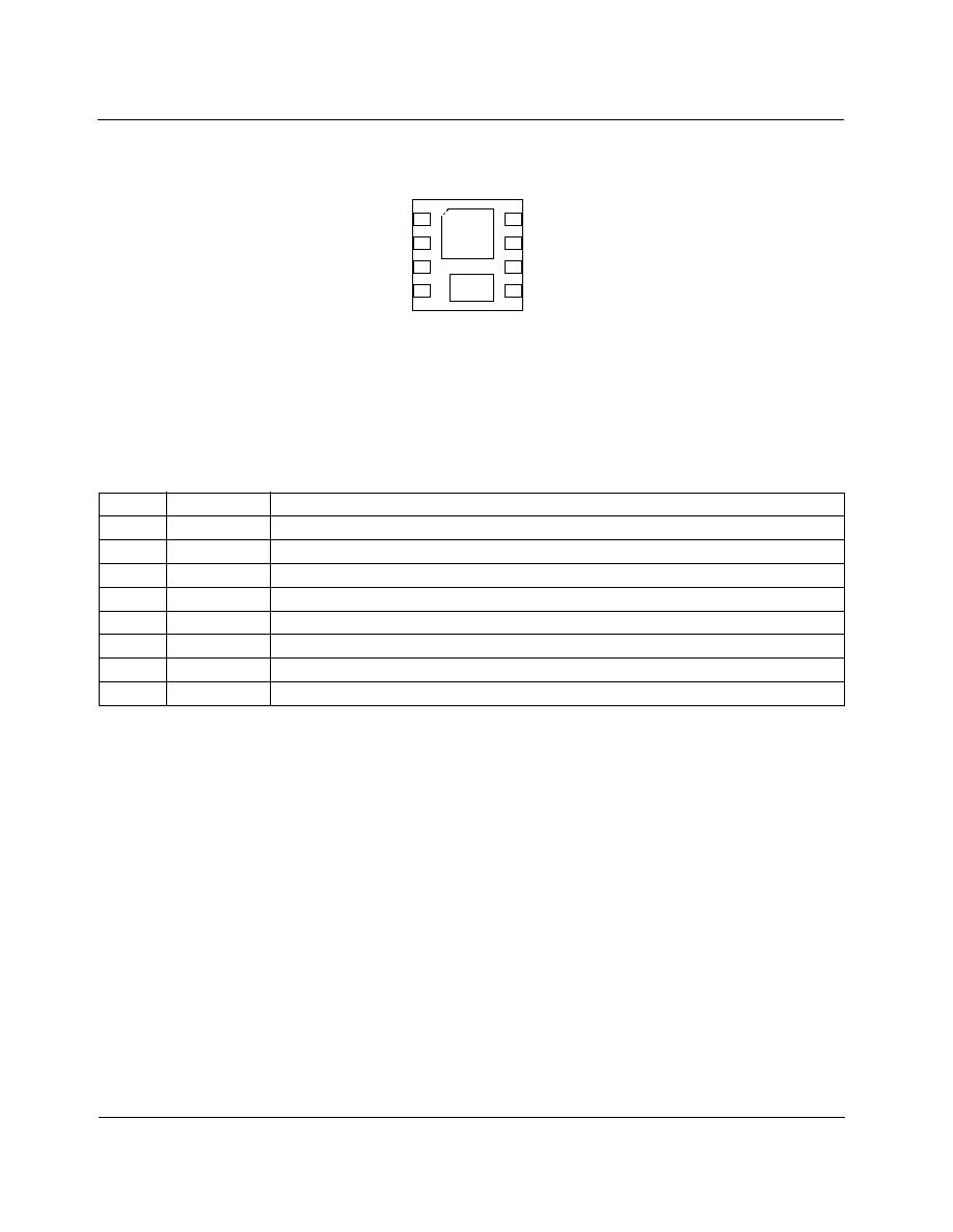
Pin Assignment
Pin Descriptions
Definition of Terms
Output Current Accuracy:
reflects the difference between the measured value of the output current (LED) and
programmed value of this current
.
Efficiency:
is expressed as a ratio between the electrical power into the LEDs and the total power consumed from the input
power supply.
Although this definition leads to a lower value than the boost converter efficiency, it more accurately reflects better system
performance, from the user's point-of-view.
Pin No.
Pin Name
Pin Function Description
1
A
DAC A Input
2
B
DAC B Input
3
CAT
LED Cathode
4
IND
Inductor
5
V
OUT
Output LED's Anode
6
GND
Ground
7
NC
No Connection
8
V
IN
Input Voltage
1
2
3
4
5
6
7
8
CAT
IND
GND
NC
A
V
IN
V
OUT
B
8-Lead 3x3mm MLP
FAN5606
Output Current Accuracy (%)
I
OUT
measured
I
OUT
programmed
≠
(
) 100
◊
I
OUT
programmed
-------------------------------------------------------------------------------------------------------------
=
Efficiency (%)
V
LED
I
LED
◊
(
) 100
◊
V
IN
I
IN
◊
---------------------------------------------------------
=

PRODUCT SPECIFICATION
FAN5606
REV. 1.0.3 1/7/05
3
Absolute Maximum Ratings
Electrical Characteristics
Recommended Operating Conditions
Notes:
1. Using Mil Std. 883E, method 3015.7 (Human Body Model) and EIA/JESD22C101-A (Charge Device Model).
2. Avoid positive polarity ESD stress at the cathode of the internal Schottky diode.
3. Multiplication Ratio is I
LED
/ I
INPUT
A
.
Parameter
Min
Typ
Max
Unit
V
IN
, A, B Voltage to GND
-0.3
6.5
V
V
OUT
, CAT Voltage to GND
-0.3
24
V
Any LED Short Circuit Duration (Anode to Cathode)
Indefinite
Lead Soldering Temperature (10 seconds)
300
∞C
Thermal Resistance
jc
8
∞C/W
Operating Junction Temperature Range
150
∞C
Storage Temperature Range
-55
150
∞C
Electrostatic Discharge (ESD) Protection (Note 1, 2)
HBM
4
kV
CDM
1
V
IN
=2.7V to 5.5V, T
A
= 25∞C, unless otherwise noted.
Parameter
Conditions
Min.
Typ.
Max.
Units
Output Current Accuracy
A = HIGH,
B = HIGH
I
NOM
= 20
mA
Efficiency (AVG)
V
IN
> 3.0V
80
%
Switching Frequency
0.5
MHz
Multiplication Ratio (Note 3)
850
1000
1150
Supply Current in OFF mode
V
A
= V
B
= 0V
0.1
µ
A
Input A Threshold
Digital
Mode
High
V
IN
-0.7
V
IN
V
Low
0
0.6
Analog Mode
1.2
Input B Threshold
Digital Mode
High
V
IN
V
Low
0
Parameter
Min
Typ
Max
Unit
Input Voltage Range
2.7
5.5
V
Operating Ambient Temperature Range
-40
25
85
∞C
Output Voltage Range
V
IN
18
V
0.9
I
NOM
◊
1.1
I
NOM
◊
0.6
V
IN
◊
0.3
V
IN
◊

FAN5606
PRODUCT SPECIFICATION
4
REV. 1.0.3 1/7/05
COIL DRIVER
DBB
START-UP
POWER GOOD
LINEAR REGULA TOR
OSC
REF
DAC
BG
V
IN
V
OUT
GND
B
A
CAT
IND
AMPLIFIER
Block Diagram
Circuit Description
When the input voltage is connected to V
IN
pin, the system is
turned on, the bandgap reference acquires its nominal volt-
age and the soft-start cycle begins. Once "power good" is
achieved (0.5mA in the diodes), the soft-start cycle stops and
the boost voltage increases to generate the desired current
selected by the input control pins.
The FAN5606 DC/DC converter automatically adjusts its
internal duty cycle to achieve high efficiency. If the output
external capacitor is shorted, the Schottky diode can be dam-
aged, therefore such a condition should be avoided.
LED Brightness Control
The inputs A and B can be digitally controlled LOW (GND)
and HIGH (V
CC
) signals. In analog mode, A input is con-
nected to an external stable voltage source via an external
resistor and B input is connected to ground. The current
flowing through the resistor is scaled by a factor of approxi-
mately 1000.
Digital Control
The FAN5606's digital decoder allows selection of the fol-
lowing modes of operation: OFF, 5mA, 10mA, 20mA per
branch.
Analog Control with PWM
In analog control mode, the LED current can go up to 25mA.
Input A is used to control the LED currents. Input B should
be connected to GND (logic level "0"). An external resistor
(R) is connected from A to a stable voltage source (V
EXTER-
NAL
) to control the LED current, I
LED
. The I
LED
is given by
the formula or the graph below:
A
0
1
0
1
B
0
0
1
1
I
LED
OFF
5mA
10mA
20mA
I
LED
V
External
V
Ref
≠
R
-----------------------------------------
Multiplication Ratio
◊
=

PRODUCT SPECIFICATION
FAN5606
REV. 1.0.3 1/7/05
5
Where
If the analog input A is driven in digital mode by an open
drain output, it is important to choose the appropriate value
of the pull-up resistor. Its resistance should be low enough to
ensure less than 0.7V dropout, hence VA > (VIN≠0.7V), as
required for HIGH logic level:
Pulse-Width-Modulation (PWM) Control
A variable duty cycle (
) can modulate any DAC input. Care
should be taken not to use a too low frequency, otherwise a
flickering effect may occur. The minimum range is 100Hz to
1KHz. For a maximum range of LED current, both A and B
inputs can be modulated at the same time.
Open Circuit Protection
A built-in over voltage protection circuit prevents the device
from being damaged when it is powered up with no load.
This circuit reduces the boost converter duty cycle, to a min-
imum thus limiting the output voltage to a safe value when
no load condition is detected. However, the FAN5606 can be
damaged when a full load (Six LEDs driven by 20mA) is
suddenly disconnected from V
OUT
. To protect the FAN5606
against this unlikely event, an external 24 V Zener diode can
be connected between V
OUT
and GND.
Shutdown Mode
The device can be disabled by applying LOW logic level
voltage to the A and B inputs. In Shutdown mode the supply
current is reduced to less than 1
µ
A.
V
Ref
1.22V
=
0
5
10
15
20
25
1.25
1.5
1.75
2
2.25
2.5
2.75
3
3.25
3.5
V
External
(V)
I
LED
(mA)
R=10Kohm
R=100kohm
Rpull-up
700mV
60
µA
------------------
<
11k
=
PWM Control
1. A is PWM Controlled, B is Low.
I
LED
(Average) =
x 5mA, where
is Duty Cycle. (Note 4
)
2. A is High and B is PWM.
I
LED
(Average) =
5mA +
x 15mA, where
is Duty Cycle.(Note 5, 6)
1KHz
1KHz
ss
ss
ss
30%
Duty Cycle
70%
Duty Cycle
A Input (PWM)
B Input (0)
ss
OFF
ILED
0mA
I
LED
(Average) = 0.3 x 5mA = 1.5mA
I
LED
(Average) = 0.7 x 5mA = 3.5mA
B Input (PWM)
1KHz
1KHz
ss
ss
ss
ss
30%
Duty Cycle
70%
Duty Cycle
A Input
ss
OFF
ILED
0mA
I
LED
(Average) = 0.3 x 20mA + 0.7 x 5mA = 9.5mA
I
LED
(Average) = 0.7 x 20mA + 0.3 x 5mA = 15.5mA