www.fairchildsemi.com
REV. 1.0.2 10/28/03
Features
∑ LED Driver for 4 Parallel-connected LEDs
∑ Low Voltage Drop (<350mV) to Support Direct Li-ion
Applications with Low V
F
LEDs
∑ Independent Control Loop for Each LED
∑ Regulated, Matched Constant Current in LEDs
∑ No External Components
∑ No EMI, No Switching Noise
∑ Built-in DAC for Digital and PWM Brightness Control
∑ Up to 91% Maximum Efficiency
∑ Up to 84mA (21mA/LED) Bias Current
∑ 2.7V to 5.5V Input Voltage Range
∑ I
CC
< 1µA in Shutdown Mode
∑ 3mmX3mm MLP-8 Package
Applications
∑ Cell Phones
∑ Handheld Computers
∑ PDA, DSC, MP3 Players
∑ LCD Display Modules
∑ Keyboard Backlight
∑ LED Displays
Description
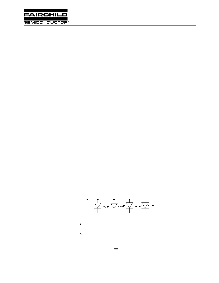
The FAN5610 generates matched current source drives for a
maximum of four LEDs. Since each LED current source has
its own self-regulating loop, precise current matching is
maintained even if there is a substantial forward voltage
spread among the LEDs. LED pre-selection therefore is not
required. In order to minimize voltage drop, and maximize
efficiency, the value of the internal current sense resistors
connected in series with the LEDs is very low (10
). This is
an important consideration for direct DC-driven white LEDs
in battery-powered systems.
The LEDs' current can be set to 0mA (OFF Mode), 7mA,
14mA, and 21mA with a built-in two-bit digital-to-analog
converter. Customized current settings can also be used.
When the control bits are set to zero, the internal circuitry is
disabled and the quiescent current drops below 1µA.
Both digital input lines (A, B) can be pulse-width-modulated
(PWM). Using PWM, any value of average LED current can
be obtained within the 1 to 20 mA range. The FAN5610 is
available in an 8-lead 3X3 MLP package.
FAN5610
LED Driver for White, Blue or any Color LED
Typical Application
D1
D2
D3
D4
V
IN
V
IN
GND
FAN5610
IN B
IN A
D
A
C
FAN5610
PRODUCT SPECIFICATION
2
REV. 1.0.2 10/28/03
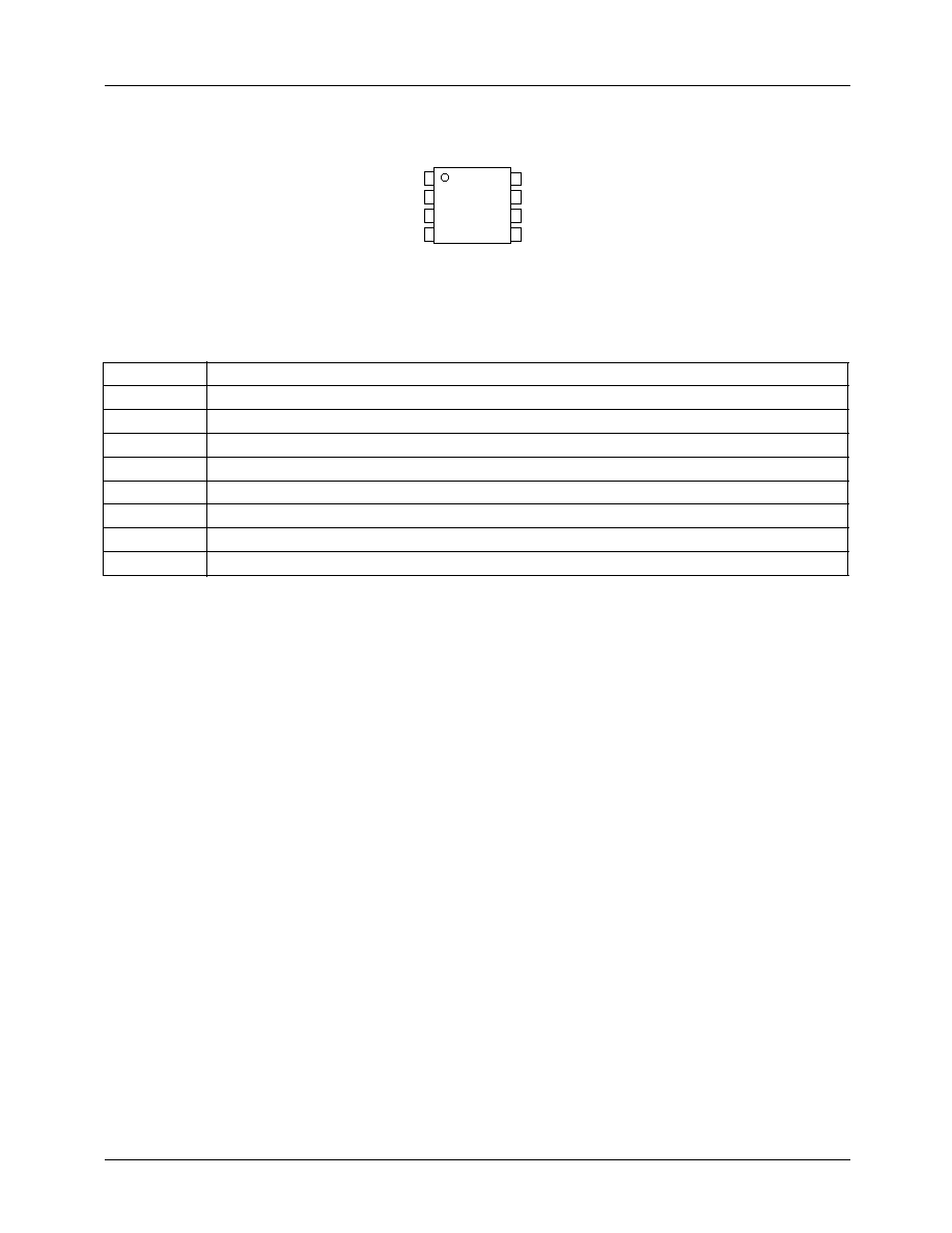
Pin Assignment
Pin Descriptions
Pin Name
Pin Function Description
D1
Cathode of Diode No.1
D2
Cathode of Diode No. 2
IN B
DAC Input B, Active High
IN A
DAC Input A, Active High
V
IN
Input Voltage
D3
Cathode of Diode No. 3
D4
Cathode of Diode No. 4
GND
Ground
IN B
IN A
V
IN
GND
D1
D2
D3
D4
3x3mm 8-LEAD MLP PACKAGE
FAN5610
PRODUCT SPECIFICATION
FAN5610
REV. 1.0.2 10/28/03
3
Absolute Maximum Ratings
Recommended Operating Conditions
DC Electrical Characteristics
Notes:
1. Using Mil Std. 883E, method 3015.7(Human Body Model) and EIA/JESD22C101-A (Charge Device Model).
2. The minimum operating voltage depends on the LED's operating voltage, as shown in the "Application Information" section.
Parameter
Min.
Max.
Unit
V
IN
,
IN A/IN B Voltage to GND
-0.3
6.0
V
Lead Soldering Temperature (10 seconds)
300
∞C
Operating Junction Temperature Range
150
∞C
Storage Temperature
-55
150
∞C
Electrostatic Discharge Protection Level (Note1)
HBM
4
kV
CDM
2
Parameter
Min.
Typ.
Max.
Unit
Input Voltage Range, V
IN
(Note2)
2.7
5.5
V
Operating Ambient Temperature Range
-40
25
85
∞C
(V
IN
=3.3V to 5.5V, T
A
= 25 ∞C, unless otherwise noted.
Boldface
values indicate specifications over the ambient
operating temperature range.)
Parameter
Conditions
Min.
Typ.
Max.
Units
Supply Current, OFF Mode
IN A = 0
IN B = 0
<1
2
µA
Output Current Accuracy
V
D
> 0.3V
IN A = 1, IN B = 1
14.8
21
26
mA
LED to LED Current Matching
V
IN
= 3.6V
IN A = 1, IN B = 1
-7.5
7.5
%
DAC Input Voltage Threshold
LOW
0
0.3
◊
V
IN
V
HIGH
0.6
◊
V
IN
V
IN
Peak Efficiency
LED V
F
=3V at 20mA
91
%
FAN5610
PRODUCT SPECIFICATION
4
REV. 1.0.2 10/28/03
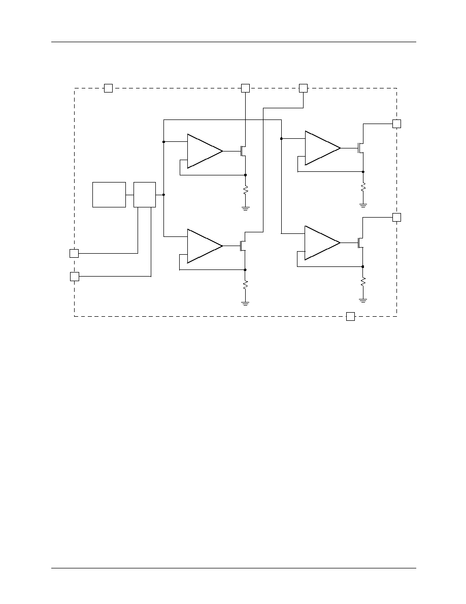
Block Diagram
GND
V
IN
+
-
Error Ampl.
+
-
Error Ampl.
+
-
Error Ampl.
+
-
Error Ampl.
D1
D2
D3
D4
2-bit
DAC
Bandgap
Reference
IN A
IN B
10
10
10
10
PRODUCT SPECIFICATION
FAN5610
REV. 1.0.2 10/28/03
5
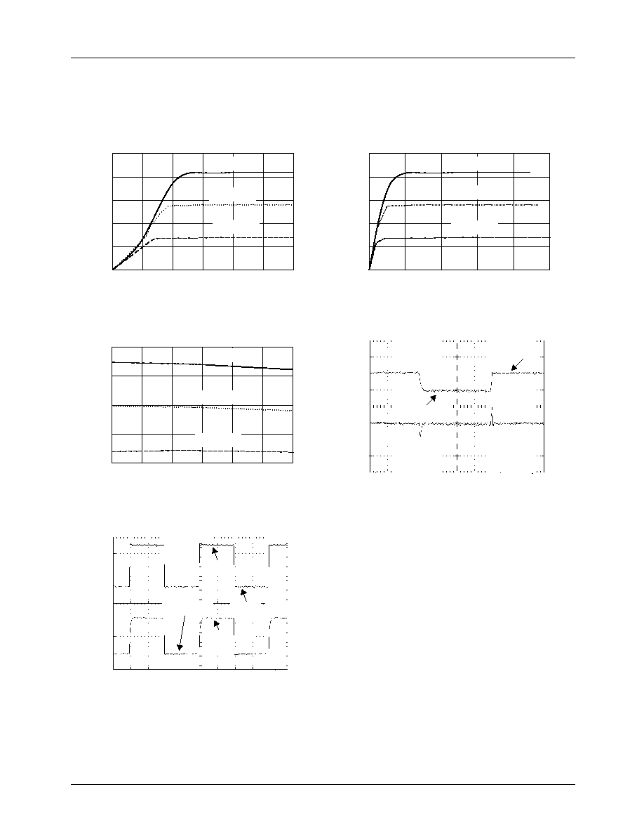
Typical Performance Characteristics
Unless otherwise specified, T
A
= 25 ∞C, using Fairchild QTLP670IW Super Bright LED.
2.5
3.0
3.5
4.0
4.5
5.0
5.5
0.0
0.5
1.0
1.5
2.0
2.5
0
5
10
15
20
25
LED Current vs. Input Voltage
(Low V
F
- White LED)
LED Current vs. Cathode Voltage
LED Current vs. Temperature
Line Transient Response
DAC Transient Response
0
5
10
15
20
25
5
10
15
20
25
Input Voltage (V)
(1V/div)
LED Current (AC)
(1mA/div)
Voltage at DAC Inputs
(2V/div)
LED Current
(10mV/div)
Ti m e (2 µs/div)
Time (50
µs/div)
V
IN
= 5V
V
IN
= 4 V
A = 1, B = 1
I
LED
= 21 m A
I
LE D
= 0m A
A = 0, B = 0
A = 1, B = 1
A = 0 , B = 1
A = 1 , B = 0
A = 1, B = 1
A = 0, B = 1
A = 1, B = 0
A = 1, B = 1
A = 0 , B = 1
A = 1 , B = 0
LED Current (mA)
LED Current (mA)
LED Current (mA)
Input Voltage (V)
-40
-20
0
20
40
60
80
Temperature (
∞C)
Cathode Voltage (V)
FAN5610
PRODUCT SPECIFICATION
6
REV. 1.0.2 10/28/03
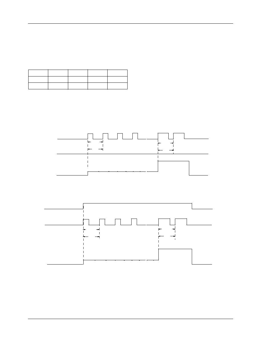
Digital Control with PWM
A is PWM and B is Low.
I
LED
(Average) =
x 7mA where
is Duty Cycle. (Note 3)
A is High and B is PWM.
I
LED
(Average) = 7mA +
x 14mA where
is Duty Cycle. (Note 4, 5)
Notes:
3. Proportionally select the duty cycle to achieve a typical LED current between 1mA to 6mA.
4. If either input A or B is high continuously, the other input can be modulated at a maximum rate of 30kHz. If this is not the
case, the maximum rate of modulation should be limited to 1kHz.
5. Proportionally select the duty cycle to achieve a typical LED current between 8mA to 20mA.
ss
A Input (PWM)
B Input (0)
ss
OFF
ILED
0mA
I
LED
(Average) = 0.7 x 7mA = 4.9mA
I
LED
(Average) = 0.3 x 7mA = 2.1mA
1KHz
30%
Duty Cycle
1KHz
70%
Duty Cycle
B Input (PWM)
ss
A Input
ss
OFF
ILED
0mA
I
LED
(Average) = 7mA + 0.7 x 14mA = 16.8mA
I
LED
(Average) = 7mA + 0.3 x 14mA = 11.2mA
1KHz
30%
Duty Cycle
1KHz
70%
Duty Cycle
Digital LED Brightness Control
1. Digital Control
A digital to analog converter selects the following modes of
operation: OFF, 7mA, 14mA, 21mA per diode. In addition,
by turning the "IN B" pin ON and OFF , the current can be
modulated between 8 to 20mA to achieve any I
average
value.
2. Digital Control with PWM
Any pin can be modulated by a variable duty cycle (
)
pulse
train. Care should be taken not to use too low frequency,
otherwise a flickering effect can be seen.The minimum range
is between 100Hz to 5KHz. For a maximum range of LED
current, both A and B can be modulated at the same time.
A
0
1
0
1
B
0
0
1
1
I
LED
OFF
7mA
14mA
21mA
PRODUCT SPECIFICATION
FAN5610
REV. 1.0.2 10/28/03
7
Digital Control with PWM
(Continued)
A and B are PWM.
I
LED
(Average) =
x 21mA where
is Duty Cycle. (Note 6)
Note:
6. Proportionally select the duty cycle to achieve the desired value of typical LED current between 1mA to 20mA.
B Input (PWM)
A Input (PWM)
ss
ss
ss
0mA
OFF
ILED
I
LED
(Average) = 0.3 x 21mA = 6.3mA
I
LED
(Average) = 0.7 x 21mA = 14.7mA
1KHz
30%
Duty Cycle
30%
Duty Cycle
1KHz
70%
Duty Cycle
70%
Duty Cycle
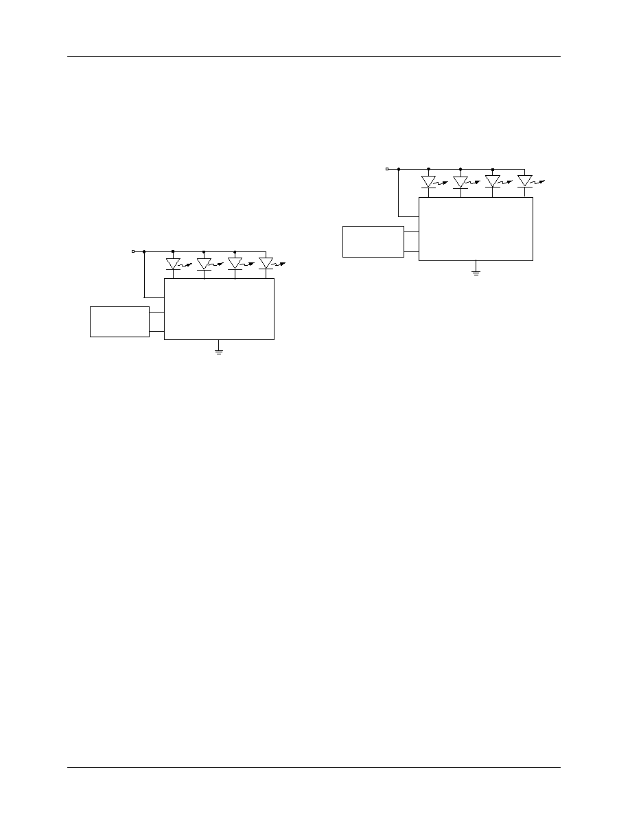
Application Information
As seen in the block diagram, the FAN5610 includes four
independent current regulators able to maintain a program-
mable constant current through LEDs, regardless of their for-
ward voltage. This is true over a wide range of input
voltage starting from V
F_max
+ 0.35V, where V
F_max
is the
highest forward voltage among the LEDs driven by
FAN5610. The independence of current (LED current
changes less than 1%) with change in V
IN
and V
F
for
V
IN
> V
F (MAX)
+ 0.35V, is shown in the graph below.
Program the LED's brightness by applying a continuous
voltage level or a PWM signal at the inputs of the built-in
digital to
a
nalog converter (DAC). When a PWM signal is
utilized to drive the DAC inputs, the current through the
LEDs is switched between two levels with the PWM signal
frequency. Consequently, the average current changes with
the duty cycle. The LED current waveform tracks the PWM
signal, so the LEDs brightness depends on the duty cycle.
For white LEDs the spectral composition is optimal at a
current level specified by the manufacturer. The DAC inputs
should be programmed to set the current required to achieve
white LED spectrum and PWM used for dimming. To main-
tain the "purest" white, the current through the LEDs should
be switched between zero and a specified current level
(usually around 20mA) corresponding to the white light
chromaticity coordinate.
Conversion errors are minimized and the best LED to LED
matching is achieved over the entire range of average current
settings, when PWM brightness control is used to modulate
the LED current between zero and the maximum value
(A=1, B=1).
Input Voltage (V)
LED Current (mA)
0
5
2.5
3.0
3.5
4.0
4.5
5.0
5.5
10
15
20
25
Current Regulation Performance
V
F2
=3 .6V
V
F1
= 3.3 V
V
IN
> V
F ( M A X)
+ 0.3 5V
FAN5610
PRODUCT SPECIFICATION
8
REV. 1.0.2 10/28/03
Application Examples:
Example 1: Drive low V
F
white or blue LEDs directly
from single cell Li-ion
When using white or blue low V
F
LEDs, and utilizing the
driver's low voltage drop, only 3.45V in V
IN
is needed for
the full 20mA LED current. Usually at 3.1V, there is still
5mA current available for the LEDs. The single cell Li-ion is
utilized in most applications like cell phones or digital still
cameras. In most cases, the Li-ion battery voltage level only
goes down to 3.0V voltage level, and not down to the full
discharge level (2.7V) before requesting the charger.
≠ V
DROP
~ 0.35V
≠ V
F (at 20mA)
< 3.1V (Low V
F
)
≠ V
IN (at 20mA)
=V
DROP
+ V
F
= 3.45V
≠ V
IN (at 5mA Typical)
~ 3.1V
Where V
IN
= Single cell Li-ion Voltage
Key advantages:
∑ No boost circuit needed for the LCD or keyboard
backlight
∑ Driver directly connected to a Li-ion battery
∑ No EMI, no switching noise, no boost efficiency lost, no
capacitor, and no inductor.
Example 2: Drive high V
F
white or blue LEDs from
existing bus from 4.0V to 5.5V
High V
F
white or blue LEDs have forward-voltage drop in
the range of 3.3V to 4.0V. To drive these LEDs with the max-
imum current of 20mA for maximum brightness, usually
requires a boost circuit for a single cell Li-ion voltage range.
In some cases, there is already a voltage bus in the system,
which can be utilized. Due to the low voltage drop of the
FAN5610, V
IN
needs to be only 350mV higher than the
voltage V
F
of LEDs connected to FAN5610.
≠ V
DROP
~ 0.35V
≠ V
F (at 20mA)
= 3.3V to 4.0V (High V
F
)
≠ V
IN(at 20mA)
V
DROP
+ V
F
= 4.35V(max)
Where V
IN
= Existing bus = 5V
Key advantages:
∑ No boost circuit needed for LCD or keyboard backlight
∑ Driver utilizes the existing bus
∑ Low voltage drop provides the full 20mA LED current at
the lowest possible voltage level.
D1
D2
D3
D4
V
IN
GND
FAN5610
IN A
IN B
Micro-Controller
V
IN
(Li-Ion)
D1
D2
D3
D4
V
IN
GND
FAN5610
IN A
IN B
Microprocessor
I/O
V
IN
(System Bus)
PRODUCT SPECIFICATION
FAN5610
REV. 1.0.2 10/28/03
9
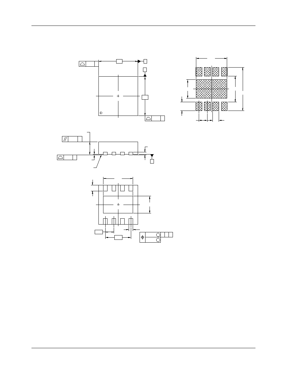
Mechanical Dimensions
3mmX3mm 8-Lead MLP Package
2X
0.15 C
2X
0.15 C
C
3.0
3.0
A
B
TOP VIEW
2.37
3.30
1.99
1.42
(0.65)
(0.20)
0.65 TYP
0.47 TYP
1
1
4
4
5
8
RECOMMENDED LAND PATTERN
0.10 C
0.08 C
1.0 MAX
0.05
0.00
SEATING
PLANE
SIDE VIEW
2.25
MAX
0.45
0.20
1.30 MAX.
0.65
1.95
8
5
BOTTOM VIEW
0.25~0.35
0.10
C A B
M
0.05
ÿ
ÿ
M
NOTES:
A. CONFORMS TO JEDEC REGISTRATION MO-229,
VARIATION VEEC, DATED 11/2001
B. DIMENSIONS ARE IN MILLIMETERS.
C. DIMENSIONS AND TOLERANCES PER
ASME Y14.5M, 1994

FAN5610
PRODUCT SPECIFICATION
10/28/03 0.0m 005
Stock#DS30005609
2003 Fairchild Semiconductor Corporation
LIFE SUPPORT POLICY
FAIRCHILD'S PRODUCTS ARE NOT AUTHORIZED FOR USE AS CRITICAL COMPONENTS IN LIFE SUPPORT DEVICES
OR SYSTEMS WITHOUT THE EXPRESS WRITTEN APPROVAL OF THE PRESIDENT OF FAIRCHILD SEMICONDUCTOR
CORPORATION. As used herein:
1. Life support devices or systems are devices or systems
which, (a) are intended for surgical implant into the body,
or (b) support or sustain life, and (c) whose failure to
perform when properly used in accordance with
instructions for use provided in the labeling, can be
reasonably expected to result in a significant injury of the
user.
2. A critical component in any component of a life support
device or system whose failure to perform can be
reasonably expected to cause the failure of the life support
device or system, or to affect its safety or effectiveness.
www.fairchildsemi.com
DISCLAIMER
FAIRCHILD SEMICONDUCTOR RESERVES THE RIGHT TO MAKE CHANGES WITHOUT FURTHER NOTICE TO
ANY PRODUCTS HEREIN TO IMPROVE RELIABILITY, FUNCTION OR DESIGN. FAIRCHILD DOES NOT ASSUME
ANY LIABILITY ARISING OUT OF THE APPLICATION OR USE OF ANY PRODUCT OR CIRCUIT DESCRIBED HEREIN;
NEITHER DOES IT CONVEY ANY LICENSE UNDER ITS PATENT RIGHTS, NOR THE RIGHTS OF OTHERS.
Ordering Information
Product Number
Package Type
Order Code
FAN5610
3x3mm 8-Lead MLP
FAN5610MPX