 | –≠–ª–µ–∫—Ç—Ä–æ–Ω–Ω—ã–π –∫–æ–º–ø–æ–Ω–µ–Ω—Ç: FAN5660 | –°–∫–∞—á–∞—Ç—å:  PDF PDF  ZIP ZIP |
www.fairchildsemi.com
REV. 1.0.2 3/28/02
Features
∑ Inverts, Doubles or Splits Input Supply Voltage
∑ 90% Typ Conversion Efficiency at 100mA load current
∑ 0.5V Typ Loss at 100mA Load
∑ Low 160µA Operating Current
∑ 5.
0
Typ Output Resistance for C1 = C2 = 100µF
∑ Selectable Oscillator Frequency: 5kHz/50kHz
∑ 8-pin SOIC package.
Applications
∑
Laptop Computers
∑
Medical Instruments
∑
Interface Power Supplies
∑
Hand-Held Instruments
∑
Operational-Amplifier Power Supplies
General Description
The FAN5660 is a monolithic charge-pump which can
invert, double or split a +1.5V to +5.5V input voltage.
Using only two identical low-cost capacitors, the charge
pump replaces switching regulators, thus eliminating
inductors and their associated cost, size, and EMI. The
device has a greater than 90% efficiency over most of its load
current range and a typical operating current of only 160µA.
The FAN5660 is ideal for both battery-powered and board-
level voltage conversion applications.
In order to enable the user optimize capacitor size and
quiescent current, the FAN5660 is offered with a frequency
control (FC) pin which selects either 5kHz or 50kHz
operation.
The Oscillator frequency can also be driven with an external
clock. The FAN5660 is available in 8-pin small-outline
packages.
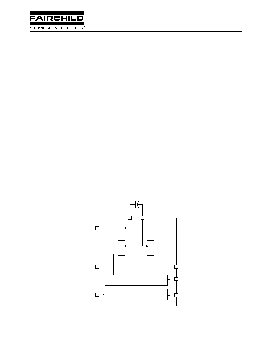
Simplified Block Diagram
VSH
LV
FC
CONTROL
OSCILLATOR
SYNC
CAP+
CAP≠
V+
VSS
FAN5660
Monolithic Inductorless CMOS DC/DC Converter
FAN5660
2
REV. 1.0.2 3/28/02
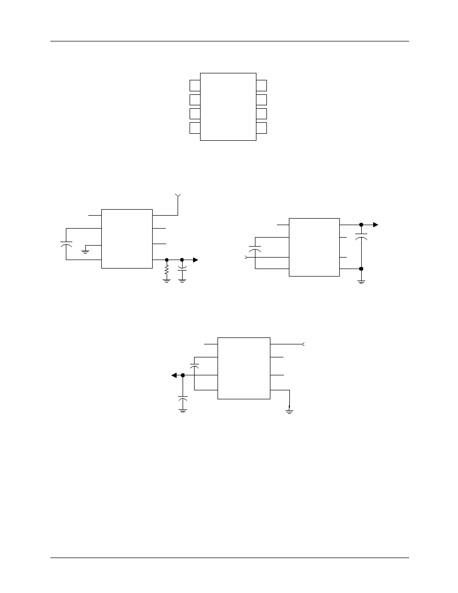
Pin Configuration
Typical Applications
Figure 1. Inverter, Test Circuit
Figure 2. Doubler
Figure 3. Splitter
1
2
3
4
8
7
6
5
FC
CAP+
VSS
CAP-
VSH
LV
SYNC
V+
SOIC
FAN5660
+
FC
CAP+
VSS
CAP-
V
IN
SYNC
LV
VSH
V+
C2
C1 = C2 = 1 to 470
µF
V
OUT
= ≠V
IN
+
C1
R
L
+V
IN
+
FC
CAP+
VSS
CAP-
SYNC
LV
VSH
V+
+
C2
V
OUT
= 2V
IN
C1 = C2 = 1 to 470
µF
C1
+
FC
CAP+
FAN5660
VSS
CAP-
V
IN
SYNC
LV
VSH
V+
C1
C2
+
V
OUT
= ≠V
IN
/2
C1 = C2 = 1 to 470
µF

FAN5660
REV. 1.0.2 3/28/02
3
Pin Definition
Pin
Number
Pin
Name
Pin Function Description
Inverter
Splitter
Doubler
1
FC
Frequency Control for Internal
Oscillator, FC open, f
OSC
= 5kHz
typ; FC = V+, f
OSC
= 50kHz typ.
FC has no effect when SYNC pin is
driven externally
Same as Inverter
Same as Inverter
2
CAP+
Charge-Pump Capacitor, Positive
Terminal
Same as Inverter
Same as Inverter
3
VSS
Power-Supply Ground Input
Power-Supply
Positive Voltage
Output
Power-Supply
Positive Voltage
Input
4
CAP-
Charge-Pump Capacitor,
Negative Terminal
Same as Inverter
Same as Inverter
5
VSH
Output, Negative Voltage
Power-Supply
Ground Input
Power-Supply
Ground Input
6
LV
Low-Voltage Operation Input.
Tie LV to VSS when input voltage is
less than 2V.
Above 2V, LV must be left open.
LV must be left open for all
input voltages
LV must be left open for
all input voltages
7
SYNC
Oscillator Control Input.
An external Oscillator may be
connected to overdrive SYNC via a
2 to 5 nF capacitor.
SYNC shall not be connected to a
low impedance DC voltage
Same as inverter, however,
do not use SYNC in
voltage-splitting mode.
Same as inverter,
however, do not use
SYNC in voltage-
doubling mode.
8
V+
Power-Supply Positive Voltage
Input
Positive Voltage Input
Positive Voltage Output
FAN5660
4
REV. 1.0.2 3/28/02
Absolute Maximum Ratings
Absolute maximum ratings are the values beyond which the device may be damaged or have its useful life
impaired. Functional operation under these conditions is not implied.
Notes
1. VSH must not be shorted to VSS or V+, even instantaeously, or device damage may result.
2. Using Mil Std. 883E, method 3015.7(Human Body Model), 400V when using JEDEC method A115-A (Machine Model).
Recommended Operating Conditions
Electrical Specifications
V+ = 5V, R
L
=
, and T
A
= +25∞C using circuit in Figure 1 with C1 = C2 = 100µF, FC and LV open, unless otherwise
specified (Note 3)
Note
3 . In the test circuit, capacitors C1 and C2 are 0.2
maximum ESR capacitors. Capacitors with higher ESR will increase output
resistance, reduce output voltage and efficiency.
Parameter
Min.
Max.
Units
Supply Voltage: V+ to VSS
-0.3
6
V
VSH Voltage to VSS
-6
0.3
V
Voltage on all other pin to VSS
-0.3
(V+) + 0.3
V
VSH and V+ Continuous Output Current (
Note 1
) 120
mA
Junction Temperature
125
∞C
Storage Temperature
-40
150
∞C
Lead Soldering Temperature, 10 seconds
300
∞C
Electrostatic Discharge Protection (
Note 2
)
4
kV
Power Dissipation (P
D
) at 85C
300
mW
Parameter
Conditions
Min.
Typ.
Max.
Units
Supply Voltage V+ to VSS or VSS to VSH
LV open
2
5.5
V
LV = VSS
1.5
2
External SYNC signal
Connected via
C =2 to 5 nF
2
V peak
to peak
Ambient Operating Temperature
T
A
-40
85
∞
C
Parameter
Symbol
Conditions
Min.
Typ.
Max.
Units
Quiescent Current
I
IN
FC open
0.16
0.5
mA
FC to V+
1
2
Output Current
I
VSH
VSH more negative than -4V
100
mA
Output Resistance
R
VSH
100mA load current
5
8
Oscillator Frequency
f
OSC
FC open
2.5
5
10
kHz
FC to V+
30
50
90
Power Efficiency
RL=1k
96
98
%
RL=0.5k
92
96
100mA load current
90
Voltage Conversion Efficiency
V
99
99.96
%

FAN5660
REV. 1.0.2 3/28/02
5
Typical Applications Diagrams
Unless otherwise specified T
A
=25∞C,V+=5V, C1=C2=100µF, Iload=0, FC and LV open, using circuit in Figure 1
1.2
1.0
FC = V+
LV to
GND
LV to
GND
FC = V+,
LV = GND
LV to GND
0.8
0.6
0.4
0.2
0
60
55
50
45
40
100
90
80
70
60
1.2
1.4
1.6
1.8
1.0
0.8
0.6
0.4
0.2
0
1
2
3
4
5
6
1.5
2
2.5
3
3.5
4
4.5
5
5.5
1
10
100
1
10
100
Supply Current vs. Supply Voltage
Supply Current vs. Oscillator Frequency
Oscillator Frequency vs.
Supply Voltage, FC to V+
Oscillator Frequency vs. Supply Voltage
Efficiency vs. Operating Frequency
Efficiency vs. Load Current
Supply Voltage (V)
Supply Voltage (V)
Operating Frequency (kHz)
1.5
2
2.5
3
3.5
4
4.5
5
5.5
Supply Voltage (V)
0
20
V+ = 1.5V
V+ = 2.5V
V+ = 3.5V
V+ = 4.5V
V+ = 5.5V
40
60
80
100
120
Load Current (mA)
Oscillator frequency (kHz)
Supply Current (mA)
Oscillator Frequency (kHz)
Efficiency (%)
1.00
0.95
0.90
0.80
0.85
0.75
0.70
Efficiency (%)
7
6
5
4
3
Oscillator Frequency (kHz)
Supply Current (mA)
FC and LV open
Iload = 10mA
Iload = 1mA
Iload = 80mA