 | –≠–ª–µ–∫—Ç—Ä–æ–Ω–Ω—ã–π –∫–æ–º–ø–æ–Ω–µ–Ω—Ç: FAN7000 | –°–∫–∞—á–∞—Ç—å:  PDF PDF  ZIP ZIP |

©2002 Fairchild Semiconductor Corporation
www.fairchildsemi.com
Rev. 1.0.5
Features
∑ Low Quiescent Current
∑ High Power Supply Ripple Rejection
∑ Low Voltage Operation
∑ A few of External Part Required
∑ Built in Power Save Switch & Mute Switch
Typical Applications
∑ Portable Compact Disk Player (DISCMAN)
∑ Portable Mini Disk Player (MD)
∑ Disc-Man
∑ MP3 Player
∑ CD-ROM
∑ Other Potable Compact Disk Media
Fan Motor Drive
Description
The FAN7000D is a monolithic integrated circuit and
suitable dual amplifier for low power.
10-SSOP-225
1
Ordering Information
Device
Package
Operating Temp.
FAN7000D
10-SSOP-225
-20
∞
C ~ +75
∞
C
FAN7000DTF
10-SSOP-225
-20
∞
C ~ +75
∞
C
FAN7000D
Low Power Amplifier

FAN7000D
2
Pin Assignments
Pin Definitions
Pin Number
Pin Name
Pin Function Description
1
PS
Power Save Switch
2
IN
A
Signal Input A
3
GND
Signal Ground
4
IN
B
Signal Input B
5
REF
Reference Voltage
6
V
CC
Supply Voltage
7
OUT
B
Signal Output B
8
GND
Power Ground
9
OUT
A
Signal Output A
10
MUTE
Mute On Switch
10
9
8
7
6
FAN7000D
1
2
3
4
5
MUTE
OUT
A
GND
OUT
B
V
CC
PS
IN
A
GND
IN
B
REF

FAN7000D
3
Internal Block Diagram
1
2
4
3
5
6
7
8
9
10
POWER SAVE SWITCH CTL
MUTE CTL
REF
REF
REF
REF
PS
IN
A
GND
IN
B
REF
V
CC
OUT
B
GND
OUT
A
MUTE
FAN7000D
4
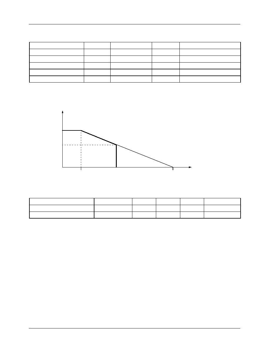
Absolute Maximum Ratings (Ta = 25
∞
∞
∞
∞
C)
Power Dissipation Curve
Recommended Operating Conditions
(Ta = 25
∞
∞
∞
∞
C)
Parameter
Symbol
Value
Unit
Remark
Maximum Supply Voltage
V
CC
4.5
V
Maximum Supply Voltage
Power Dissipation
P
D
300
mW
Power Dissipation
Operating Temperature
T
OPR
-20 ~ +75
∞
C
Operating Temperature
Storage Temperature
T
STG
-55 ~ +125
∞
C
Storage Temperature
Thermal Resistance
T
ja
150
∞
C/W
-
Parameter
Symbol
Min.
Typ.
Max.
Unit
Operating Supply Voltage
V
CC
1.8
3.0
4.0
V
Recommended Load
R
L
16
-
32
Power dissipation (mW)
300
150
25
75
125
Ambient temperature, Ta (
∞
C)

FAN7000D
5
Electrical Characteristics
(R
L
= 16
, Rg = 600
, Ta = 25
∞
C)
Parameter
Symbol
Conditions
Min.
Typ.
Max.
Unit
Quiescent Current 1
I
CC1
V
CC
= 2.4V
-
5.5
10.0
mA
Quiescent Current 2
I
CC2
V
CC
= 4.5V, Mute = GND
-
1.0
2.0
mA
Quiescent Current 3
I
CC3
V
CC
= 4.5V, PS = GND
-
-
1.0
µ
A
Close Loop Voltage Gain 1
G
VC1
V
CC
= 2.4V, f = 1kHz,
V
O
= -10dBm
30
32
34
dB
Close Loop Voltage Gain 2
G
VC1
V
CC
= 1.8V, f = 1kHz,
V
O
= -20dBm
29
32
34
dB
Channel Balance 1
G
V1
V
CC
= 2.4V, f = 1kHz,
V
O
= -10dBm
-
-
1.0
dB
Channel Balance 2
G
V2
V
CC
= 1.8V, f = 1kHz,
V
O
= -20dBm
-
-
1.0
dB
Total Harmonic Distortion
THD
V
CC
= 2.0V, f = 1kHz,
P
O
= 1mW
-
0.5
1.5
%
Ripple Rejection Ratio
RR
V
CC
= 1.8V, f = 100Hz,
Rg = 1k
, V
R
= -20dBm,
BPF = 100Hz
43
60
-
dB
Crosstalk
CT
V
CC
= 2.4V, f = 100Hz,
Rg = 1k
, V
O
= -10dB
43
50
-
dB
Output Noise Voltage
V
NOISE
V
CC
= 4.5V, Rg = 1k
,
BPF = 20Hz ~ 20kHz
-
60
100
µ
Vrms
Output Power
P
OUT
V
CC
= 3.0V, f = 1kHz,
THD = 10%
20
40
-
mW
PS Attenuation Ratio
ATT
PS
V
CC
= 1.8V, f = 100Hz,
PS = GND, V
IN
= -10dB
-
-
-80
dB
MUTE Attenuation Ratio
ATT
MU
V
CC
= 1.8V, f = 100Hz,
MUTE = GND, V
IN
= -10dB
-
-
-80
dB
PS ON Input Current
I
PSON
V
CC
= 1.5V, V
REF
0.85V
-
0.2
1.0
µ
A
MUTE OFF Input Current
I
MOFF
V
CC
= 1.5V, V
REF
0.85V
-
0.2
1.0
µ
A
PS ON High Level
V
HPS
V
CC
= 1.5V, V
REF
0.85V
0.5
0.65
-
V
MUTE OFF High Level
V
HMU
V
CC
= 1.5V, V
REF
0.85V
0.5
0.65
-
V

FAN7000D
6
Application Information
1. PS Block
This block diagram describes the power save switch circuits.
The drive block is controlled by PS pin, which can be derived from micro controller.
It controls bias of the internal circuits of FAN7000D, so that it makes FAN7000D operate when input voltage level reaches
high level.
2. Mute Block
The block diagram describes the mute on switch circuits.
The drive block is controlled by MUTE pin, which can be derived from micro controller.
When the pin of mute turns on, it makes reference voltage of internal circuits approximately 0V, so that it keeps the device of
FAN7000D off.
3. AMP Block
This block diagram describes the AMP block with resistances, which control gain of FAN7000D.
The gain of FAN7000D is
Output voltage of FAN7000D can be 40 times as much as input voltage, so it eliminates the number of external circuits and
offers headphone input.
4. Popping
Noise Reduction
If PS pin (Pin1 , Power save switch) connect the micro controller, the micro controller must follow the same sequence 1 in
order to reduce popping noise on mute mode.
PS on
Mute on
PS off
Mute operation
PS on
Mute off
Normal operation (Sequence 1) If PS connect
V
CC
, the micro controller follow the sequence 2.
Mute on
Mute Operation
Mute off
Normal operation (Sequence 2)
V
OUT
V
IN
--------------
40 32 dB
[
]

FAN7000D
7
Test Circuits
1
2
3
4
5
10
9
8
7
6
PS
IN
A
GND
IN
B
REF
Vcc
OUT
B
GND
OUT
A
MUT
E
F
A
N
7
0
0
0
D
A
PS_SW
MUTE_SW
220uF
0.1uF
0.1uF
220uF
4.7
4.7
16
16
16
16
16
16
16
16
DC
RIPPLE
1
2
3
4
2
1
4
3
1
2
1
2
22uF
Rg
Rg
V
1
R
L
R
L
4.7uF
I
1
V
10
I
10

FAN7000D
8
Typical Application Circuits
1
2
3
4
5
10
9
8
7
6
PS
IN
A
GND
IN
B
REF
Vcc
OUT
B
GND
OUT
A
MUT
E
F
A
N
7
0
0
0
D
PS_SW
V
DC
220uF
0.1uF
0.1uF
220uF
4.7
4.7
OFF
ON
22uF
V
R
4.7uF
OFF
ON
R-ch
L-ch
V
R
Sg
1
Sg
2
4.7uF
4.7uF
FAN7000D
9
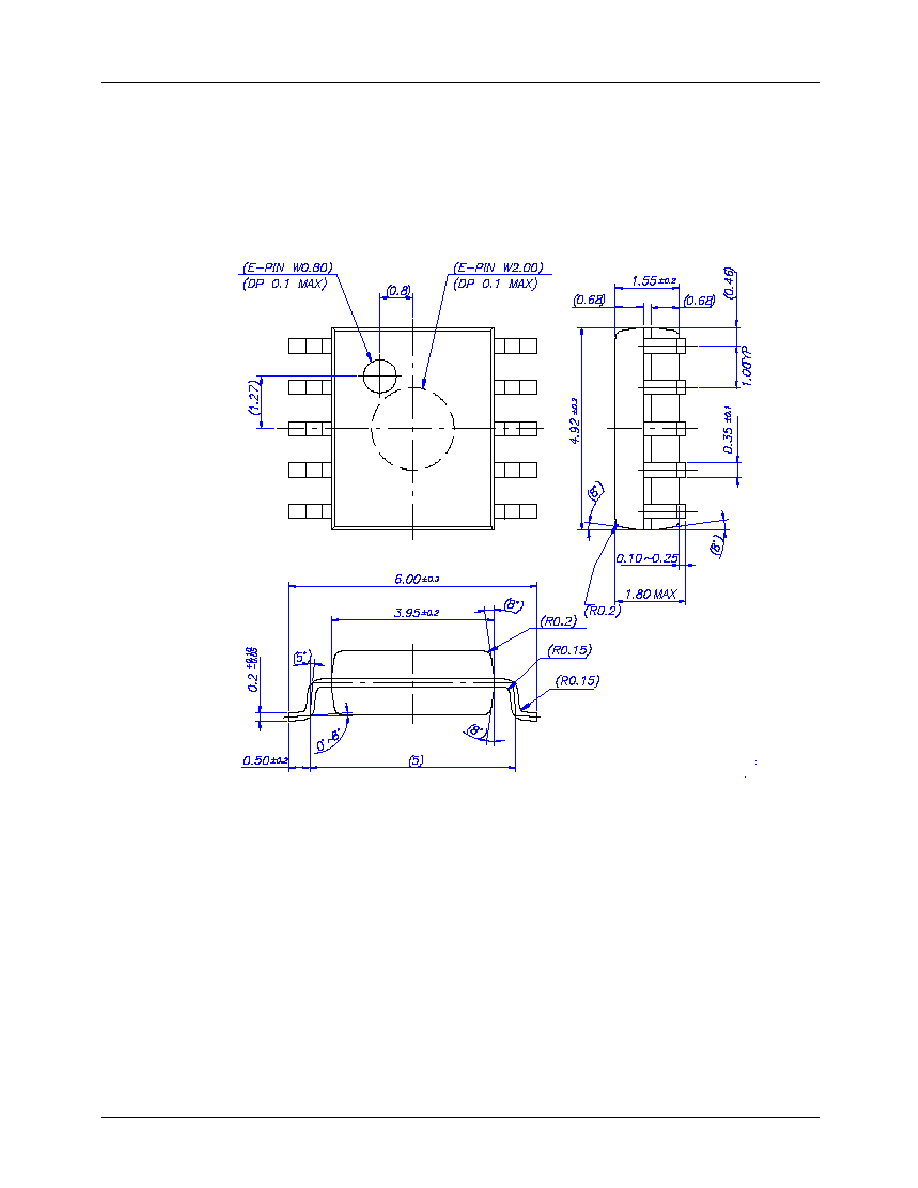
Package Dimensions
10-SSOP-225

FAN7000D
7/16/02 0.0m 001
Stock#DSxxxxxxxx
2002 Fairchild Semiconductor Corporation
LIFE SUPPORT POLICY
FAIRCHILD'S PRODUCTS ARE NOT AUTHORIZED FOR USE AS CRITICAL COMPONENTS IN LIFE SUPPORT DEVICES
OR SYSTEMS WITHOUT THE EXPRESS WRITTEN APPROVAL OF THE PRESIDENT OF FAIRCHILD SEMICONDUCTOR
CORPORATION. As used herein:
1. Life support devices or systems are devices or systems
which, (a) are intended for surgical implant into the body,
or (b) support or sustain life, and (c) whose failure to
perform when properly used in accordance with
instructions for use provided in the labeling, can be
reasonably expected to result in a significant injury of the
user.
2. A critical component in any component of a life support
device or system whose failure to perform can be
reasonably expected to cause the failure of the life support
device or system, or to affect its safety or effectiveness.
www.fairchildsemi.com
DISCLAIMER
FAIRCHILD SEMICONDUCTOR RESERVES THE RIGHT TO MAKE CHANGES WITHOUT FURTHER NOTICE TO ANY
PRODUCTS HEREIN TO IMPROVE RELIABILITY, FUNCTION OR DESIGN. FAIRCHILD DOES NOT ASSUME ANY
LIABILITY ARISING OUT OF THE APPLICATION OR USE OF ANY PRODUCT OR CIRCUIT DESCRIBED HEREIN; NEITHER
DOES IT CONVEY ANY LICENSE UNDER ITS PATENT RIGHTS, NOR THE RIGHTS OF OTHERS.