 | –≠–ª–µ–∫—Ç—Ä–æ–Ω–Ω—ã–π –∫–æ–º–ø–æ–Ω–µ–Ω—Ç: FAN7021 | –°–∫–∞—á–∞—Ç—å:  PDF PDF  ZIP ZIP |

©2002 Fairchild Semiconductor Corporation
www.fairchildsemi.com
Rev. 1.0.1
Features
∑ Continuous Average Power is 1.0W (8
)
∑ Low THD: Under 0.2% (5V)
∑ Do not Need Output Coupling Capacitor or Bootstrap
Capacitor
∑ Low Shutdown Current: 0.01
µ
A
∑ Shutdown: High Active
∑ Built in Reduction Circuit for Popping noise
∑ Built in TSD Circuit
Typical Applications
∑ Cellular Phone
∑ Portable Computer
∑ Audio Systems
Description
The FAN7021 is a bridge connected audio power amplifier
capable of delivering 1W of continuous average power to an
8
load with less than 0.2%(THD) from a 5V power supply.
The FAN7021 require few external components and operate
on low supply voltage from 2.0V to 5.5V. Since the
FAN7021 does not require output coupling capacitor,
bootstrap capacitors, or snubber networks, it is ideally suited
for low power portable systems that require minimum
volume and weight. The FAN7021 feqtures an externally
controlled, low power consumption shutdown mode (0.01
uA,typ). Additional FAN7021 features include thermal
shutdown protection, unity gain stability, and external gain
set.
8-SOP-225
1
Internal Block Diagram
5
Bias
20k
8
3
4
2
1
6
100k
100k
7
20k
IN-
IN+
BP
VDD
SD
GND
V
O2
V
O1
FAN7021
CMOS Power Amplifier

FAN7021
2
Pin Assignments
Pin Definitions
Absolute Maximum Ratings (Ta = 25
∞
∞
∞
∞
C)
Recommended Operating Conditions
(Ta = 25
∞
∞
∞
∞
C)
Pin Number
Pin Name
Pin Function Description
1
SD
Shutdown
2
BP
Bypass
3
IN+
Input +
4
IN
-
Input
-
5
V
O1
Power AMP Output 1
6
V
DD
Supply Voltage
7
GND
Ground
8
V
O2
Power AMP Output 2
Parameter
Symbol
Value
Unit
Remark
Maximum Supply Voltage
V
DD
6.0
V
Maximum Supply Voltage
Power Dissipation
P
D
-
W
-
Operating Temperature
T
OPR
-
40 ~ +85
∞
C
Operating Temperature
Storage Temperature
T
STG
-
65 ~ +150
∞
C
Storage Temperature
Thermal Resistance
JA
180
∞
C/W
Thermal Resistance
Parameter
Symbol
Min.
Typ.
Max.
Unit
Operating Supply Voltage
V
DD
2.0
-
5.5
V
8
7
6
5
FAN7021
1
2
3
4
V
O2
GND
V
DD
V
O1
SD
BP
IN+
IN-

FAN7021
3
Electrical Characteristics
(R
L
= 8
, Ta = 25
∞
C,
Unless otherwise specified)
Parameter
Symbol
Conditions
Min.
Typ. Max. Unit
V
DD
= 5.0V, UNLESS OTHERWISE SPECIFIED
Quiescent Power Supply Current
I
DD
V
IN
=0V,I
O
=0A
-
4.0
7.0
mA
Shutdown Current
I
SD
V
SD
=V
DD
-
0.01
2.0
µ
A
Output Offset Voltage
V
OS
V
IN
=0V
-
5
50
mV
Output Power
P
O
THD=0.2% (Max.);f=1KHz
-
1
-
W
Total Harmonic Distortion+noise
THD+N
P
O
=0.25Wrms,A
VD
=2
f=1KHz
-
0.1
-
%
f=20KHz
-
0.4
-
%
Power Supply Rejection Ratio
PSRR
V
DD
=4.9V to 5.1V
-
65
-
dB
V
DD
= 3.3V, UNLESS OTHERWISE SPECIFIED
Quiescent Power Supply Current
I
DD
V
IN
=0V,I
O
=0A
-
3.0
-
mA
Shutdown Current
I
SD
V
SD
=V
DD
-
0.01
-
µ
A
Output Offset Voltage
V
OS
V
IN
=0V
-
5
-
mV
Output Power
P
O
THD=1% (Max.);f=1KHz
-
0.5
-
W
Total Harmonic Distortion+noise
THD+N
P
O
=0.25Wrms,A
VD
=2
f=1KHz
-
0.15
-
%
f=20KHz
-
0.45
-
%
Power Supply Rejection Ratio
PSRR
V
DD
=3.2V to 3.4V
-
65
-
dB
V
DD
= 2.6V, UNLESS OTHERWISE SPECIFIED
Quiescent Power Supply Current
I
DD
V
IN
=0V,I
O
=0A
-
2.5
-
mA
Shutdown Current
I
SD
V
SD
=V
DD
-
0.01
-
µ
A
Output Offset Voltage
V
OS
V
IN
=0V
-
5
-
mV
Output Power
P
O
THD=0.3% (Max.);f=1KHz
-
0.25
-
W
Total Harmonic Distortion+Noise
THD+N
P
O
=0.25Wrms,A
VD
=2
f=1KHz
-
0.25
-
%
f=20KHz
-
0.5
-
%
Power Supply Rejection Ratio
PSRR
V
DD
=2.5V to 2.7V
-
65
-
dB

FAN7021
4
Typical Application Circuits
+
V
DD
C
S
10uF
R
PU
10K
+
C
B
1uF
+
C
I
0.47uF
R
I
20K
R
F
20K
GND
Bias
SD
V
DD
BP
IN+
IN-
V
O1
V
O2
4
3
2
6
1
7
8
5
20K
20K
100K
100K
Speaker
8
FAN7021
5
Performance Characteristics
100
1k
10k
0.01
0.1
1
10
VDD=5V
Po=1W
RL=8
THD
[
%
]
Frequency [Hz]
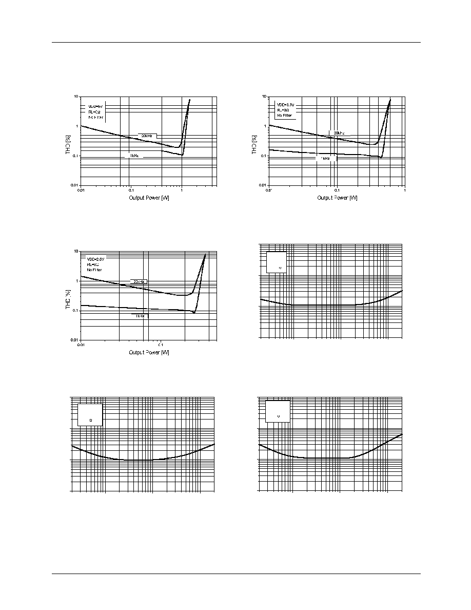
Figure 2. THD+N versus output power
Figure 3. THD+N versus output power
Figure 5. THD+N versus Frequency
Figure 1. THD+N versus output power
Figure 6. THD+N versus Frequency
100
1k
10k
0.01
0.1
1
10
VDD=3.3V
Po=250mW
RL=8
TH
D [
%
]
Frequency [Hz]
100
1k
10k
0.01
0.1
1
10
VDD=2.6V
Po=250mW
RL=8
T
HD [
%
]
Frequency [Hz]
Figure 4. THD+N versus Frequency