©2003 Fairchild Semiconductor Corporation
www.fairchildsemi.com
Rev. 1.0.1
Features
∑ 1.85W
RMS
and 2.45W
RMS
Power Per Each Channel Into
4
Load With Less Than 1% and 10% THD+N,
Respectively
∑ Selectable Gain Via Internal Gain Control Circuit Which
Eliminates External Gain Setting Resistors : 6dB, 10.3dB,
15.6dB, 21.6dB(Select)
∑ Low Quiescent Current : Typical 5.5mA@5V
∑ Low Shutdown Current : Typical 0.04
µA@5V
∑ Fully Differential Input, Which Immunes the Common
Mode Noise
∑ Stereo Headphone Drive
∑ Active Low Shutdown Logic
∑ Guaranteed Stability Under No Load Condition
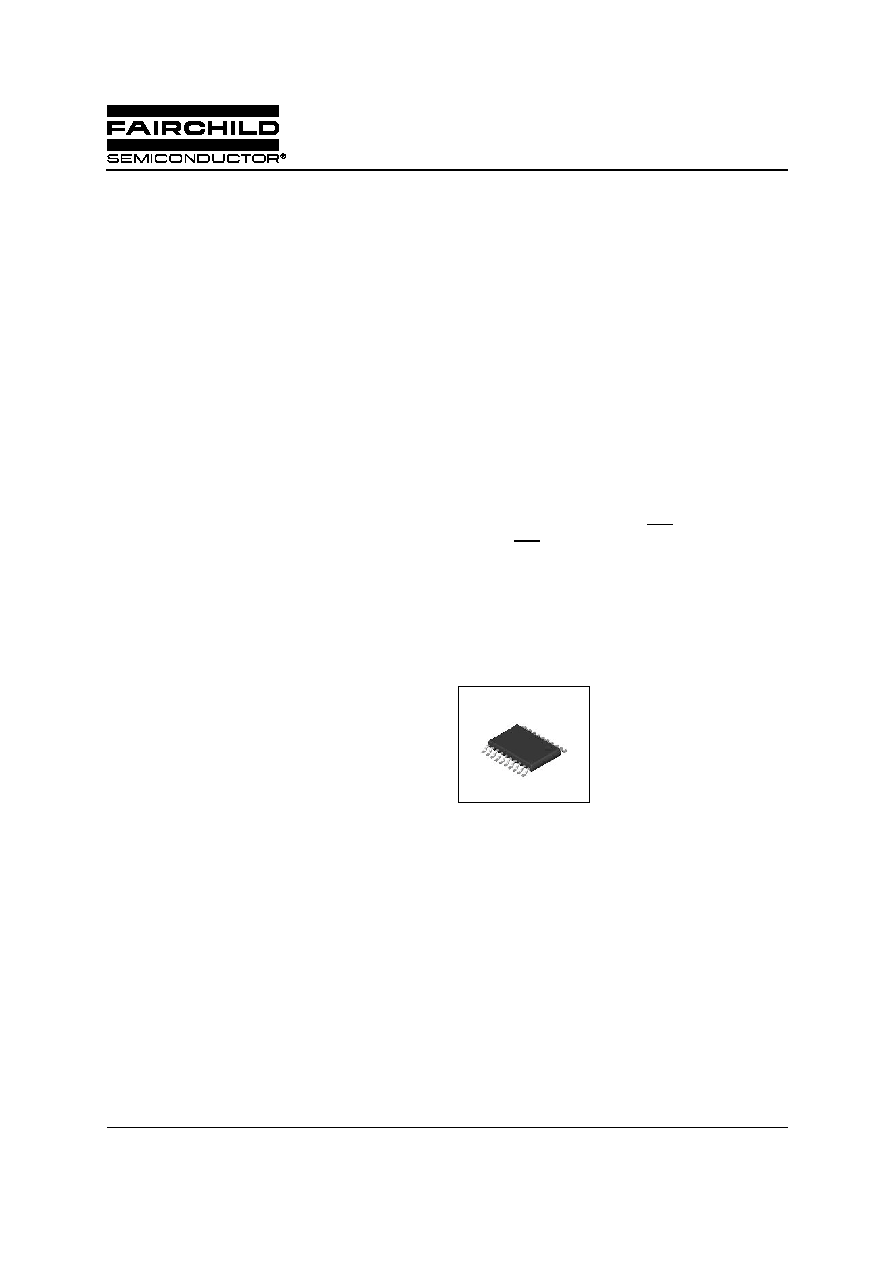
∑ Thermally Enhanced Surface-Mount 20TSSOP-EP
Package
Description
The FAN7031 is a dual fully differential power amplifier in a
20-pin TSSOP-EP thermally enhanced package. When
delivering 1.85W of continuous RMS power into 4
speaker
at 5V supply, the FAN7031 has less than 1% of THD+N over
the entire audible frequency range, 20Hz to 20kHz. To save
power consumption in the portable applications, the
FAN7031 provides shutdown function. Setting the shutdown
pin to ground level, the FAN7031 falls into shutdown mode
and consumes less than 4
µA over all supply voltage range,
2.7V to 5.5V. Two gain setting pins(G0 and G1) control the
gain of the FAN7031. The gain is selectable to 6dB, 10dB,
15.6dB and 21.6dB. The FAN7031 provides the single-
ended(SE) operation by setting SE/BTL pin to above V
DD
/2.
Using SE/BTL pin and a mechanical switch which provides
at the headphone jack, SE mode and BTL mode are automat-
ically determined. Additional components such as resistors
for gain setting and bootstrap capacitors are not needed,
making the FAN7031 well suited for portable sound systems
and other hand-held sound equipment. Target applications
include notebook and desktop computers and portable audio
equipment.
20-TSSOP-EP
1
FAN7031
2W Stereo Power Amplifier with Four Selectable
Gain Setting and Headphone Drive

FAN7031
2
Internal Block Diagram
Gain Control
SE/BTL
Control
On/Off
Con
tro
l
TSD
VDD/2
Current
Source
CONTROL
BIAS
BYPASS
ROUT+
ROUT-
RIN-
RIN+
G0
SD
SE/BTL
LIN-
LIN+
LOUT+
LOUT-
G1

FAN7031
3
Pin Assignments
Pin Description
* All GND is internally tied together.
** For the best performance, VDD, PVDD1 and PVDD2 must be the same voltage level(strongly recommend).
Pin No
Symbol
I/O
Decription
1*
GND
-
Ground
2
G0
I
Gain Selection Input(MSB)
3
G1
I
Gain Selection Input(LSB)
4
LOUT+
O
Left Channel (+) Output
5
LIN-
I
Left Channel (-) Input
6**
PVDD2
I
Left Channel Power Supply Voltage
7
RIN+
I
Right Channel (+) Input
8
LOUT-
O
Left Channel (-) Output
9
LIN+
I
Left Channel (+) Input
10
BYPASS
O
Bypass Capacitor Connect
11*
GND
-
Ground
12
SE/BTL
I
Single-Ended & BTL Selection:
GND
SE/BTL VDD/2:BTL Mode
VDD/2 < SE/BTL
VDD: SE Mode
13
NC
-
No Connection
14
ROUT-
O
Right Channel (-) Output
15**
PVDD1
I
Right Channel Power Supply Voltage
16**
VDD
I
Power Supply Voltage
17
RIN-
I
Right Channel (-) Input
18
ROUT+
O
Right Channel (+) Output
19
SD
I
Shutdown Logic Low
SD=VDD: Chip Enable
SD=GND: Chip Shutdown
20*
GND
-
Ground
GND
G0
G1
LOUT+
LIN-
PVDD2
RIN+
LOUT-
LIN+
BYPASS
GND
SD
ROUT+
RIN-
VDD
PVDD1
ROUT-
NC
SE/BTL
GND
Heat Sink
1
10
11
20

FAN7031
4
Absolute Maximum Ratings
Note1 : Rthja was derived using a JEDEC multi layer and single layer.
Operating Ratings
Parameter
Symbol
Value
Unit
Remark
Maximum Supply Voltage
VDDmax
6.0V
V
Power Dissipation
P
D
Internally Limited
W
See Derating Curve
Operating Temperature
T
OPG
-40 ~ +85
∞C
Storage Temperature
T
STG
-65 ~ +150
∞C
Junction Temperature
T
J
150
∞C
Thermal Resistance
(Junction to Ambient)
Rthja
30.4
∞C/W
Multi Layer Board
112.5
Single Layer Board
ESD Rating (Human Body Model)
2000
V
Parameter
Symbol
Min
Typ
Max
Unit
Power Supply Voltage
V
DD
2.7
-
5.5
V

FAN7031
5
Electrical Characteristics
(V
DD
= 5.0V, Ta = 25
∞C, unless otherwise specified)
Electrical Characteristics
(Continued)
(V
DD
= 3.3 V, Ta = 25
∞C, unless otherwise specified)
Electrical Characteristics
(Continued)
(V
DD
= 2.7 V, Ta = 25
∞C, unless otherwise specified)
Parameter
Symbol
Conditions
Min.
Typ. Max.
Unit
Offset Voltage
V
OFF
RL=4
, Av=6dB
-25
-
25
mV
Supply Current
I
DD
No Input, No Load
-
5.5
10
mA
Shutdown Current
I
SD
SD = GND
-
0.04
4
µA
Output Power
P
O
THD+N =1%, RL = 4
, f = 1kHz
-
1.85
-
W
THD+N =10%, RL = 4
, f = 1kHz
-
2.45
-
W
BTL Mode Gain
Av
SE/BTL=GND, G0=GND, G1=GND,
Vin=4Vpp, No Load
-
6
-
dB
SE/BTL=GND, G0=GND, G1=VDD,
Vin=2.44Vpp, No Load
-
10.3
-
dB
SE/BTL=GND, G0=VDD, G1=GND,
Vin=1.34Vpp, No Load
-
15.6
-
dB
SE/BTL=GND, G0=VDD, G1=VDD,
Vin=0.66Vpp, No Load
-
21.3
-
dB
SE Mode Gain
SE/BTL=VDD,
Vin=2.44Vpp, No Load
-
4.3
-
dB
Total Harmonic Distortion + Noise
THD+N
P
O
= 1W, RL=4
, f = 20kHz
-
0.2
0.75
%
Power Supply Rejection Ratio
PSRR
C
byp
= 0.47
µF, RL=4, BTL Mode,
VDD=500mVpp, f = 1kHz
40
70
-
dB
Parameter
Symbol
Conditions
Min.
Typ. Max.
Unit
Offset Voltage
V
OFF
RL=4
, Av=6dB
-25
-
25
mV
Supply Current
I
DD
No Input, No Load
-
4.3
8
mA
Shutdown Current
I
SD
SD = GND
-
0.08
4
µA
Output Power
P
O
THD+N =10%, RL = 4
, f=1kHz
-
1.02
-
W
Total Harmonic Distortion + Noise
THD+N
P
O
= 0.5W, RL = 4
, f = 20kHz
-
0.2
0.75
%
Power Supply Rejection Ratio
PSRR
C
byp
= 0.47
µF, RL=4, BTL Mode,
VDD=330mVpp, f = 1kHz
40
70
-
dB
Parameter
Symbol
Conditions
Min.
Typ. Max.
Unit
Offset Voltage
V
OFF
RL=4
, Av=6dB
-25
-
25
mV
Supply Current
I
DD
No Input, No Load
-
4.1
7
mA
Shutdown Current
I
SD
SD = GND
-
0.04
4
µA
Output Power
P
O
THD+N =10%, RL = 4
, f=1kHz
-
0.54
-
W
Total Harmonic Distortion + Noise
THD+N
P
O
= 0.25W, RL = 4
, f = 20kHz
-
0.2
0.75
%
Power Supply Rejection Ratio
PSRR
C
byp
= 0.47
µF, RL=4, BTL Mode,
VDD=270mVpp, f = 1kHz
-
65
-
dB