
©2003 Fairchild Semiconductor Corporation
www.fairchildsemi.com
Rev. 1.0.0
Features
∑ 1.9W
RMS
and 2.45W
RMS
Power Per Each Channel Into
4
Load With Less Than 1% and 10% THD+N,
Respectively
∑ Internally Fixed Gain : 21.6dB(Av=12)
∑ Low Quiescent Current : Typical 5.5mA@5V
∑ Low Shutdown Current : Typical 0.04
µA@5V
∑ Fully Differential Input, Which Immunes the Common
Mode Noise
∑ Active Low Shutdown Logic
∑ Guaranteed Stability Under No Load Condition
∑ Very Small Volume and Thermally Enhanced Surface-
Mount 14MLP Package(4mm*4mm)
Typical Applications
∑ Cellular Phones
∑ Notebook Computer
∑ Desktop Computer
Description
The FAN7033MP is a dual fully differential power amplifier
in a thermally enhanced 14-pin MLP package. When deliv-
ering 1.9W of continuous RMS power into 4
speaker at 5V
supply, the FAN7033MP has less than 1% of THD+N over
the entire audible frequency range, 20Hz to 20kHz. To save
power consumption in the portable applications, the
FAN7033MP provides shutdown function. Setting the shut-
down pin to ground level, the FAN7033MP falls into shut-
down mode and consumes less than 4
µA over all supply
voltage range, 2.7V to 5.5V. Additional components such as
resistors for gain setting and bootstrap capacitors are not
needed, making the FAN7033MP well suited for portable
sound systems and other hand-held sound equipments. Tar-
get applications include the cellular phones, notebook, desk-
top computers, etc.
14MLP
1
BOTTOM VIEW
FAN7033MP
2W Stereo Power Amplifier with Fixed Gain
Internal Block Diagram
RIN-
LIN+
LIN-
ROUT+
ROUT-
BYPASS
LOUT+
LOUT-
BIAS
&
CONTROL
VDD
GND
VDD/2
6
12
13
9
11
7
8
1
5
SD 14
10 PVDD1
3 PVDD2
90k
90k
90k
15k
15k
15k
15k
90k
90k
90k
90k
90k
15k
15k
15k
15k
RIN+ 4
2

FAN7033MP
2
Pin Assignments
Pin Descriptions
* Pin8(GND) and Exposed PAD are internally tied together.
**For the best performance, VDD, PVDD1 and PVDD2 must be the same voltage level(strongly recommend).
Pin No
Symbol
I/O
Decription
1
LOUT+
O
Left Channel (+) Output
2
LIN-
I
Left Channel (-) Input
3**
PVDD2
I
Left Channel Power Supply Voltage
4
RIN+
I
Right Channel (+) Input
5
LOUT-
O
Left Channel (-) Output
6
LIN+
I
Left Channel (+) Input
7
BYPASS
O
Bypass Capacitor Connect
8*
GND
-
Ground
9
ROUT-
O
Right Channel (-) Output
10**
PVDD1
I
Right Channel Power Supply Voltage
11**
VDD
I
Power Supply Voltage
12
RIN-
I
Right Channel (-) Input
13
ROUT+
O
Right Channel (+) Output
14
SD
I
Shutdown Logic Low
SD=VDD: Device Enable
SD=GND: Device Shutdown
BOTTOM VIEW
1
2
3
4
5
6
7
14
13
12
11
10
9
8
TOP VIEW
1
2
3
4
5
6
7
14
13
12
11
10
9
8

FAN7033MP
3
Absolute Maximum Ratings
* Rthja was derived using the JEDEC boards.
Operating Rating
Parameter
Symbol
Value
Unit
Remark
Maximum Supply Voltage
VDDmax
6.0V
V
Power Dissipation
P
D
Internally Limited
W
Operating Temperature
T
OPG
-40 ~ +85
∞C
Storage Temperature
T
STG
-65 ~ +150
∞C
Junction Temperature
T
Jmax
150
∞C
Thermal Resistance
(Junction to Ambient)
Rthja*
38
∞C/W
Multi-Layer
145
Single-Layer
ESD Rating (Human Body Model)
2000
V
ESD Rating (Machine Model)
300
V
Parameter
Symbol
Min.
Typ.
Max.
Unit
Power Supply Voltage
V
DD
2.7
-
5.5
V
FAN7033MP
4
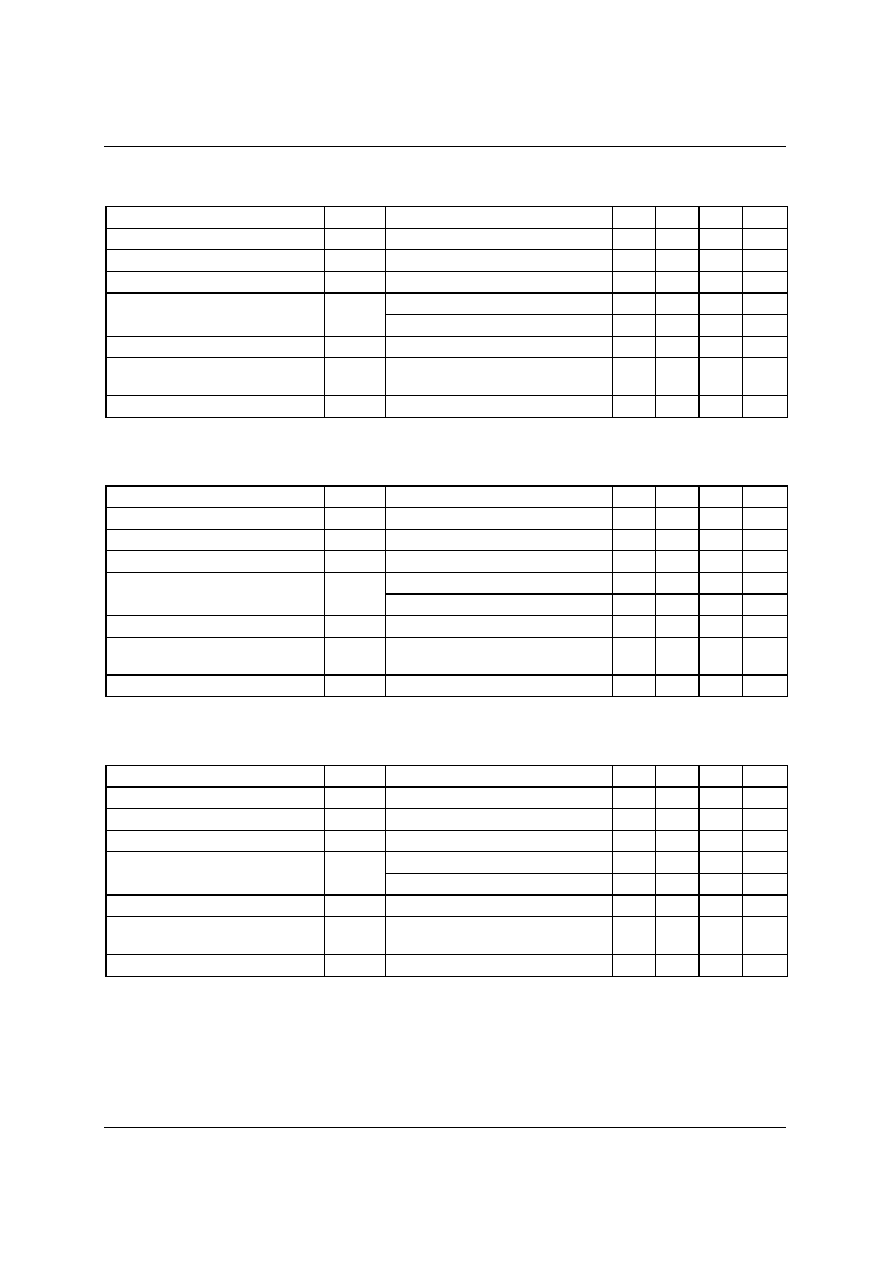
Electrical Characteristics
(V
DD
= 5.0V, Ta = 25
∞C, unless otherwise specified)
Electrical Characteristics
(V
DD
= 3.3 V, Ta = 25
∞C, unless otherwise specified)
Electrical Characteristics
(V
DD
= 2.7 V, Ta = 25
∞C, unless otherwise specified)
Parameter
Symbol
Conditions
Min.
Typ. Max.
Unit
Offset Voltage
V
OFF
RL=4
, Av=21.6dB
-25
-
25
mV
Supply Current
I
DD
No Input, No Load
-
5.5
10
mA
Shutdown Current
I
SD
SD = GND
-
0.04
4
µA
Output Power
P
O
THD+N =1%, RL = 4
, f = 1kHz
-
1.9
-
W
THD+N =1%, RL = 8
, f = 1kHz
-
1.25
-
W
Total Harmonic Distortion + Noise
THD+N
P
O
= 1W, RL=4
, f = 20kHz
-
0.6
-
%
Power Supply Rejection Ratio
PSRR
C
byp
= 1
µF, RL=4, BTL Mode,
VDD=500mVpp, f = 1kHz
38
68
-
dB
Output Noise Voltage
VN
Input=GND, RL=4
, f=1kHz
-
-120
-
dBv
Parameter
Symbol
Conditions
Min.
Typ. Max.
Unit
Offset Voltage
V
OFF
RL=4
, Av=21.6dB
-25
-
25
mV
Supply Current
I
DD
No Input, No Load
-
4.5
8
mA
Shutdown Current
I
SD
SD = GND
-
0.04
4
µA
Output Power
P
O
THD+N =1%, RL = 4
, f = 1kHz
-
0.75
-
W
THD+N =1%, RL = 8
, f = 1kHz
-
0.53
-
W
Total Harmonic Distortion + Noise
THD+N
P
O
= 1W, RL=4
, f = 20kHz
-
0.75
-
%
Power Supply Rejection Ratio
PSRR
C
byp
= 1
µF, RL=4, BTL Mode,
VDD=330mVpp, f = 1kHz
38
68
-
dB
Output Noise Voltage
VN
Input=GND, RL=4
, f=1kHz
-
-120
-
dBv
Parameter
Symbol
Conditions
Min.
Typ. Max.
Unit
Offset Voltage
V
OFF
RL=4
, Av=21.6dB
-25
-
25
mV
Supply Current
I
DD
No Input, No Load
-
4.1
7
mA
Shutdown Current
I
SD
SD = GND
-
0.04
4
µA
Output Power
P
O
THD+N =1%, RL = 4
, f = 1kHz
-
0.45
-
W
THD+N =1%, RL = 8
, f = 1kHz
-
0.32
-
W
Total Harmonic Distortion + Noise
THD+N
P
O
= 0.5W, RL=4
, f = 20kHz
-
0.9
-
%
Power Supply Rejection Ratio
PSRR
C
byp
= 1
µF, RL=4, BTL Mode,
VDD=270mVpp, f = 1kHz
36
62
-
dB
Output Noise Voltage
VN
Input=GND, RL=4
, f=1kHz
-
-120
-
dBv
