 | –≠–ª–µ–∫—Ç—Ä–æ–Ω–Ω—ã–π –∫–æ–º–ø–æ–Ω–µ–Ω—Ç: FAN7040MX | –°–∫–∞—á–∞—Ç—å:  PDF PDF  ZIP ZIP |

©2004 Fairchild Semiconductor Corporation
www.fairchildsemi.com
Rev. 1.1.0
Features
∑ DC Volume Control : +37dB ~ -52dB
∑ Few External Components
∑ Mute Mode
∑ Thermal Protection
∑ Short-Circuit Proof
∑ No Switch-On or Switch-Off Clicks
∑ Good Overall Stability
∑ Low Power Consumption
∑ Low HF Radiation
∑ ESD Protected On All Pins
Applications
∑ TVs and Monitors
∑ Portable Computers
∑ Desktop computers
∑ Low Voltage Audio Systems
Description
The FAN7040 is a mono Bridge-Tied Load(BTL) output
amplifier with DC volume control. It is designed for use in
TVs and monitors, but is also suitable for battery-fed porta-
ble recorders and radios. The device is contained in a 20-lead
small outline package.
A Missing Current Limiter(MCL) is built in. the MCL cir-
cuit is activated when the difference in current between the
output terminal of each amplifier exceeds 130mA. This level
of 130mA allows for Single-Ended(SE) headphone applica-
tions.
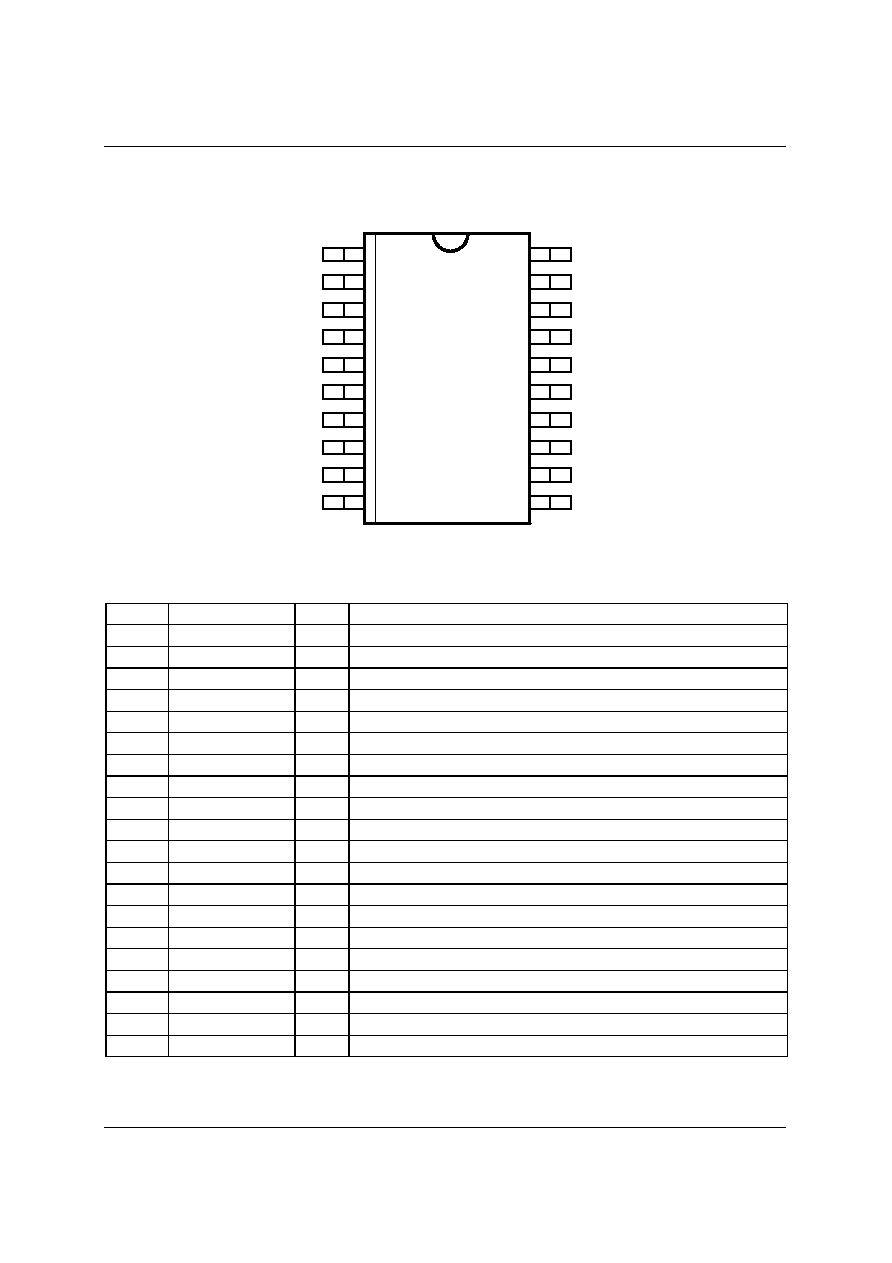
20SOP
1
FAN7040
3W Mono BTL Amplifier with DC Volume Control
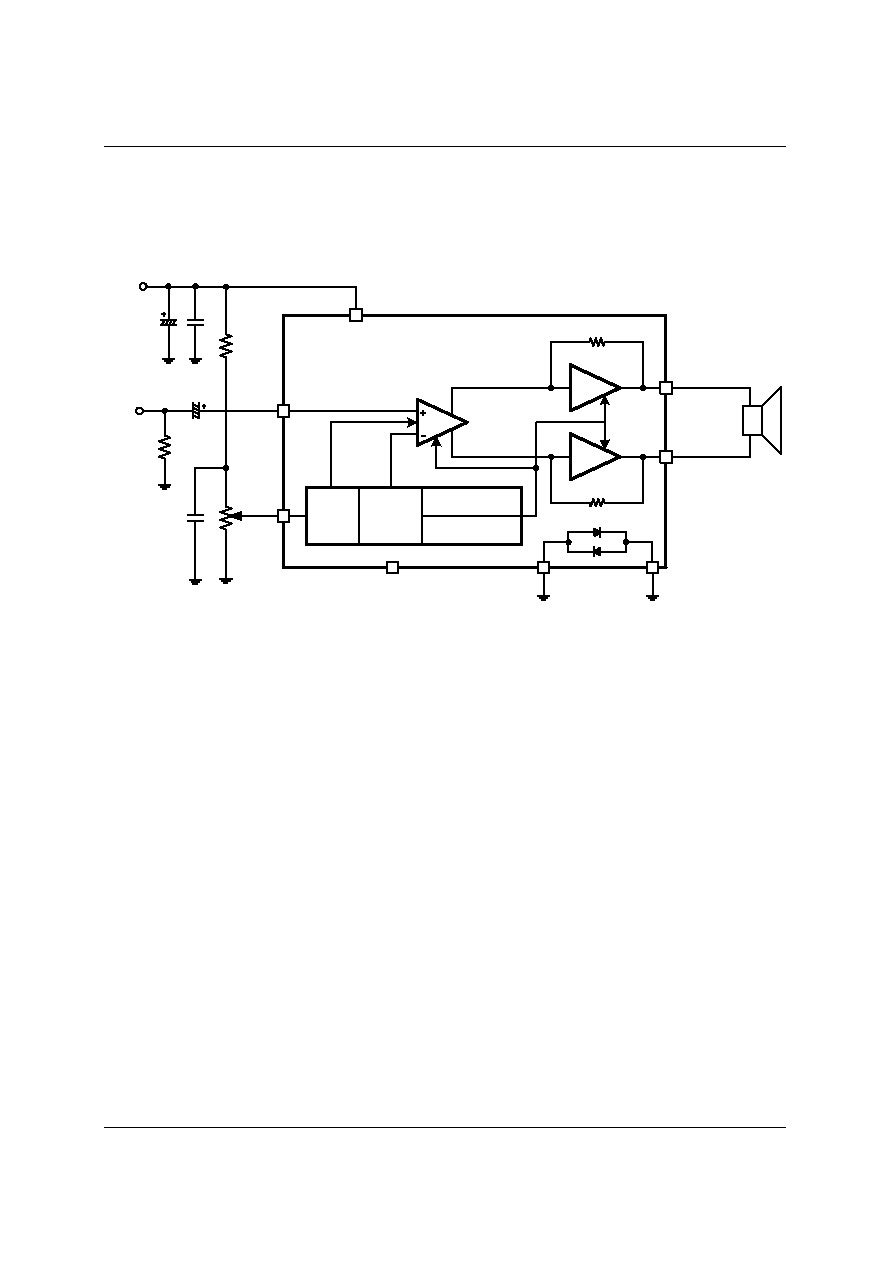
Internal Block Diagram
Over-Temperature
Protection
Missing current
protection
Bandgap
Reference
DC Gain
Control
VGA
Power Amp
Power Amp
5
7
14
17
15
1-3, 8-13, 16, 18 and 20
6
4
IN
VC
NC
SGND
PGND
OUT-
OUT+
FAN7040
VCC
FAN7040
2
Pin Assignments
Pin Description
Pin No
Symbol
I/O
Description
1
N.C.
No Connection
2
N.C.
No Connection
3
N.C.
No Connection
4
V
CC
I
Positive Power Supply
5
IN
I
Signal Input
6
SGND
Signal Ground
7
VC
I
DC Volume Control
8
N.C.
No Connection
9
N.C.
No Connection
10
N.C.
No Connection
11
N.C.
No Connection
12
N.C.
No Connection
13
N.C.
No Connection
14
OUT+
O
Positive Output
15
PGND
Power Ground
16
N.C.
No Connection
17
OUT-
O
Negative Output
18
N.C.
No Connection
19
N.C.
No Connection
20
N.C.
No Connection
FAN7040
1
10
11
20

FAN7040
3
Absolute Maximum Ratings
Operating Ratings
Parameter
Symbol
Value
Unit
Remark
Maximum Supply Voltage
V
CCmax
18
V
Maximum Input Voltage
V
PIN5
, V
PIN7
5.0
V
Repetitive Peak Output Current
I
ORM
1.25
A
Non-repetitive Peak Output Current
I
OSM
1.5
A
Power Dissipation
P
D
Internally Limited
W
Storage Temperature
T
STG
-55 ~ +150
∞C
Junction Temperature
T
J
150
∞C
Thermal Resistance
Rthj-a
70
∞C/W
Parameter
Symbol
Min
Typ
Max
Unit
Power Supply Voltage
V
CC
4.5
-
18
V
Operating Temperature
T
OPG
-40
-
+85
∞C

FAN7040
4
Electrical Characteristics
(V
CC
= 12V, Ta = 25
∞C, R
L
=16
, unless otherwise specified)
Notes
1. With a load connected to the outputs, the quiescent current will increase as much as the DC output offset voltage divided by R
L
.
2. The maximum gain of the amplifier is normally reached at VC=1.4V typical.
.
Parameter
Symbol
Conditions
Min.
Typ. Max.
Unit
Supply Current
I
CC
V
i
=0V, No Load
-
5
10
mA
Maximum Gain(VC=2V)
Note 2
Output Power
P
O
THD+N =10%, R
L
=16
3
3.5
-
W
Total Harmonic Distortion
THD
P
O
= 0.5W
-
0.3
1
%
Maximum Total Voltage Gain
G
V,max
34
37
-
dB
Input Signal Handling(RMS)
V
i,rms
VC=0.8V, THD<1%
0.6
0.7
-
Vrms
Noise Output Voltage
V
n(o)
f=1kHz, Rs=0
-
15
-
µV
Power Supply Rejection Ratio
PSRR
Vripple=200mV, Rs=0
, f=1kHz
30
-
-
dB
DC Output Offset Voltage
V
OS
|(OUT+)-(OUT-)|, VC=1.4V
-
-
210
mV
Input Impedance(pin3)
Z
I
15
20
25
k
Minimum Gain(VC=0.5V)
Minimum Total Voltage Gain
G
V,min
-65
-52
-40
dB
Noise Output Voltage
V
n(o)
f=1kHz, Rs=0
-
1
-
µV
Mute Position
Output Voltage in Mute Position
V
o,mute
VC=0.3V, V
I
=600mVrms,
f=1kHz
-
1
-
µV
DC Volume Control
Voltage Gain Control Range
G
V
|G
V,max
|+|G
V,min
|
-
89
-
dB
Control Current
I
VC
VC=0V
50
62
75
µA
note1

FAN7040
5
Performance Characteristics
-100
+0
-90
-80
-70
-60
-50
-40
-30
-20
-10
20
100k
50
100
200
500
1k
2k
5k
10k
20k
50k
Frequency [Hz]
PSRR [d
B]
VC=0.5V, Rs=5k
VC=2V, Rs=5k
VC=2V, Rs=0
-100
+0
-90
-80
-70
-60
-50
-40
-30
-20
-10
20
100k
50
100
200
500
1k
2k
5k
10k
20k
50k
Frequency [Hz]
PSRR [d
B]
VC=0.5V, Rs=5k
VC=2V, Rs=5k
VC=2V, Rs=0
Fig. 1 Supply Current
Fig. 2 Power Supply Rejection Ratio
0.01
30
0.02
0.05
0.1
0.2
0.5
1
2
5
10
20
10m
10
20m
50m
100m
200m
500m
1
2
5
Output Power [W]
T
HD+N [
%
]
VCC=12V
VC=2V
f=1kHz
R
L
=16
BW<22kHz
0.01
30
0.02
0.05
0.1
0.2
0.5
1
2
5
10
20
10m
10
20m
50m
100m
200m
500m
1
2
5
Output Power [W]
T
HD+N [
%
]
VCC=12V
VC=2V
f=1kHz
R
L
=16
BW<22kHz
VCC=12V
VC=2V
f=1kHz
R
L
=16
BW<22kHz
Fig. 3 THD+N vs. Output Power
Fig. 4 THD+N vs. Frequency
0.0
0.2
0.4
0.6
0.8
1.0
1.2
1.4
1.6
1.8
2.0
-80
-60
-40
-20
0
20
40
VCC=12V
Ga
in [
d
B
]
DC Volume Control Voltage [V]
0.0
0.2
0.4
0.6
0.8
1.0
1.2
1.4
1.6
1.8
2.0
-80
-60
-40
-20
0
20
40
VCC=12V
Ga
in [
d
B
]
DC Volume Control Voltage [V]
Fig. 5 Gain vs. DC Volume Control
Fig. 6 Input Signal Handling
0
4
8
12
16
20
0.0
1.0m
2.0m
3.0m
4.0m
5.0m
6.0m
7.0m
VCC=12V
VC=2V
S
upp
l
y
Cur
r
e
nt
[
A
]
Supply Voltage [V]
No load
0
4
8
12
16
20
0.0
1.0m
2.0m
3.0m
4.0m
5.0m
6.0m
7.0m
VCC=12V
VC=2V
S
upp
l
y
Cur
r
e
nt
[
A
]
Supply Voltage [V]
No load
2
4
6
8
10
12
14
16
18
20
0.3
0.4
0.5
0.6
0.7
0.8
0.9
1.0
Inp
u
t
V
o
l
t
a
g
e
[
V
r
m
s]
Power Supply [V]
VCC=12V
VC=0.8V
R
L
=16
THD+N=1%
2
4
6
8
10
12
14
16
18
20
0.3
0.4
0.5
0.6
0.7
0.8
0.9
1.0
Inp
u
t
V
o
l
t
a
g
e
[
V
r
m
s]
Power Supply [V]
VCC=12V
VC=0.8V
R
L
=16
THD+N=1%
0.01
10
0.02
0.05
0.1
0.2
0.5
1
2
5
20
20k
50
100
200
500
1k
2k
5k
10k
Frequency [Hz]
T
HD+N [
%
]
VCC=12V
VC=2V
R
L
=16
BW<80kHz
0.01
10
0.02
0.05
0.1
0.2
0.5
1
2
5
20
20k
50
100
200
500
1k
2k
5k
10k
Frequency [Hz]
T
HD+N [
%
]
VCC=12V
VC=2V
R
L
=16
BW<80kHz

FAN7040
6
Performance Characteristics
(continued)
Fig. 7 Control Current vs. DC Volume Control
Fig. 8 Power Dissipation vs Supply Voltage
Fig. 9 Power Dissipation vs. Supply Voltage
Fig. 10 Power Dissipation vs. Output Power
Fig. 11 Output Power vs. Supply Voltage
Fig. 12 Output Power vs. Supply Voltage
0.0
0.4
0.8
1.2
1.6
2.0
-80
-60
-40
-20
0
20
40
60
VCC=12V
Cur
r
en
t I
[
µ
A]
DC Volume Control Voltage[V]
0.0
0.4
0.8
1.2
1.6
2.0
-80
-60
-40
-20
0
20
40
60
VCC=12V
Cur
r
en
t I
[
µ
A]
DC Volume Control Voltage[V]
3
0
4
8
12
16
20
0
1
2
Pow
e
r Dissi
patio
n
[W]
Power Supply [V]
VCC=12V
f=1kHz
THD+N <1%
R
L
=8
R
L
=16
R
L
=25
0
4
8
12
16
20
0
1
2
Pow
e
r Dissi
patio
n
[W]
Power Supply [V]
VCC=12V
f=1kHz
THD+N <1%
R
L
=8
R
L
=16
R
L
=25
0
4
8
12
16
20
0
1
2
3
VCC=12V
f=1kHz
THD+N <10%
P
o
w
e
r Di
ss
i
p
a
t
i
on [W]
Power Supply [V]
R
L
=8
R
L
=16
R
L
=25
0
4
8
12
16
20
0
1
2
3
VCC=12V
f=1kHz
THD+N <10%
P
o
w
e
r Di
ss
i
p
a
t
i
on [W]
Power Supply [V]
R
L
=8
R
L
=16
R
L
=25
0.0
0.5
1.0
1.5
2.0
2.5
3.0
0.0
0.2
0.4
0.6
0.8
1.0
1.2
1.4
1.6
1.8
2.0
2.2
2.4
2.6
2.8
3.0
VCC=12V
VC=2V
THD+N < 1%
Po
w
e
r D
i
s
s
i
pa
tio
n
[
W
]
Output Power [W]
R
L
=8
R
L
=16
R
L
=25
0.0
0.5
1.0
1.5
2.0
2.5
3.0
0.0
0.2
0.4
0.6
0.8
1.0
1.2
1.4
1.6
1.8
2.0
2.2
2.4
2.6
2.8
3.0
VCC=12V
VC=2V
THD+N < 1%
VCC=12V
VC=2V
THD+N < 1%
Po
w
e
r D
i
s
s
i
pa
tio
n
[
W
]
Output Power [W]
R
L
=8
R
L
=16
R
L
=25
2
4
6
8
10
12
14
16
18
20
0
1
2
3
4
5
6
f=1kHz
BW<22KHz
1% THD+N
O
u
t
put P
o
w
e
r
[
W
]
Power Supply [VCC]
R
L
=8
R
L
=16
R
L
=25
2
4
6
8
10
12
14
16
18
20
0
1
2
3
4
5
6
f=1kHz
BW<22KHz
1% THD+N
f=1kHz
BW<22KHz
1% THD+N
O
u
t
put P
o
w
e
r
[
W
]
Power Supply [VCC]
R
L
=8
R
L
=16
R
L
=25
2
4
6
8
10
12
14
16
18
20
0
1
2
3
4
5
6
7
8
O
u
t
put P
o
w
e
r
[
W
]
Power Supply [VCC]
f=1kHz
BW<22KHz
10% THD+N
R
L
=8
R
L
=16
R
L
=25
2
4
6
8
10
12
14
16
18
20
0
1
2
3
4
5
6
7
8
O
u
t
put P
o
w
e
r
[
W
]
Power Supply [VCC]
f=1kHz
BW<22KHz
10% THD+N
f=1kHz
BW<22KHz
10% THD+N
R
L
=8
R
L
=16
R
L
=25

FAN7040
7
Performance Characteristics
(continued)
Fig. 15 Power Derating Curve
Fig. 14 Output Voltage in Mute State
40n
100u
100n
200n
500n
1u
2u
5u
10u
20u
50u
20
20k
50
100
200
500
1k
2k
5k
10k
Frequency [Hz]
Ou
tp
ut
V
o
lta
g
e
[
V
]
VCC=12V
R
L
=16
VC=0.5V
VC=2V
40n
100u
100n
200n
500n
1u
2u
5u
10u
20u
50u
20
20k
50
100
200
500
1k
2k
5k
10k
Frequency [Hz]
Ou
tp
ut
V
o
lta
g
e
[
V
]
VCC=12V
R
L
=16
VCC=12V
R
L
=16
VC=0.5V
VC=0.5V
VC=2V
VC=2V
40n
10u
100n
200n
500n
1u
2u
5u
20
20k
50
100
200
500
1k
2k
5k
10k
Frequency [Hz]
O
u
t
p
u
t
V
o
l
t
ag
e
[
V
]
VCC=12V
VC=0.3V
Vin=600mV
40n
10u
100n
200n
500n
1u
2u
5u
20
20k
50
100
200
500
1k
2k
5k
10k
Frequency [Hz]
O
u
t
p
u
t
V
o
l
t
ag
e
[
V
]
VCC=12V
VC=0.3V
Vin=600mV
VCC=12V
VC=0.3V
Vin=600mV
0
25
50
75
100
125
150
0.0
0.2
0.4
0.6
0.8
1.0
1.2
1.4
1.6
1.8
2.0
P
DMAX
=1.79W
Po
w
e
r
D
i
ss
i
p
ati
o
n
[W
]
Ambient Temperature [
O
C]
0
25
50
75
100
125
150
0.0
0.2
0.4
0.6
0.8
1.0
1.2
1.4
1.6
1.8
2.0
P
DMAX
=1.79W
Po
w
e
r
D
i
ss
i
p
ati
o
n
[W
]
Ambient Temperature [
O
C]
Fig. 15 Output Noise Voltage
FAN7040
8
Typical Application Circuit
Over-Temperature
Protection
Missing current
protection
Bandgap
Reference
DC Gain
Control
VGA
Power Amp
Power Amp
5
7
14
17
15
1-3, 8-13, 16, 18 and 20
6
4
IN
VC
NC
SGND
PGND
OUT-
OUT+
FAN7040
VCC
Signal Input
R
L
=16
22k
82k
100nF
220
µF
0.47
µF
R
S
Vi
V
CC
100nF
5k

FAN7040
9
Typical Application Information
Functional Description
The FAN7040 is a mono BTL output amplifier with DC volume control. It is designed for use in TVs and monitors but is also
suitable for battery-fed portable recorders and radios.
In conventional DC volume circuits the control or input stage is AC-coupled to the output stage via external capacitors to keep
the offset voltage low. In the FAN7040 the DC volume control stage is integrated into the input stage so that no coupling
capacitors are required. With this configuration, a low offset voltage is still maintained and the minimum supply voltage
remains low.
The BTL principle offers the following advantages:
∑Lower peak value of the supply current
∑The frequency of the ripple on the supply voltage is twice the signal frequency.
Consequently, a reduced power supply with smaller capacitors can be used which also results in cost reductions. For portable
applications there is a trend to decrease the supply voltage, resulting in a reduction of output power at conventional output
stages. Using the BTL principle increases the output power. The maximum gain of the amplifier is fixed at 37dB. The DC vol-
ume control stage has a logarithmic control characteristic. The total gain can be controlled from 37dB to -52dB. If the DC vol-
ume control voltage is below 0.3V, the device switches to the mute mode. The amplifier is short-circuit proof to ground, Vcc
and across the load. A thermal protection circuit is also implemented. If the crystal temperature rises above +150∞C the TSD is
operated, thereby the output power is off. Special attention is given to switch-on and switch-off clicks, low HF radiation and a
good overall stability.
Voltage Gain
The maximum closed-loop voltage gain has been internally fixed at 37dB.
Output Power
The output power as a function of supply voltage has been measured at THD=10%. The maximum output power is limited by
the maximum allowed power dissipation at Ta=25∞C approximately 1.8W, and the maximum available output current is 1.25A
repetitive peak current.
Short Circuit Protection
The output (pins 14 and 17) can be short-circuited to ground respectively to +VDD. The Missing Current Limiter(MCL) pro-
tection circuit will shut-off the amplifier. Removing the short-circuit will reset the amplifier automatically. Short-circuit across
the load(pins 14 and 17) will activate the thermal protection circuit; this will result in thermal shutdown protection.
For single-end application the output peak current may not exceed 130mA; at higher output currents the short circuit protec-
tion(MCL) will be activated.
Power Dissipation
Power dissipation is a major concern when designing any power amplifier and must be thoroughly understood to ensure a suc-
cessful design. Equation (1) states the maximum power dissipation point for a bridged amplifier operating at a given supply
voltage and driving a specified output load.
Since the FAN7040 is driving a bridged amplifier, the internal maximum power dissipation point of the FAN7040 results from
equation (1). Even with the large internal power dissipation, the FAN7040 does not require heat sinking over a wide range of
ambient temperature. From equation (1), assuming a 12V power supply and a 16
load, the maximum power dissipation point
is 1.8W. The maximum power dissipation point obtained from equation (1) must not be greater than the power dissipation that
results from equation (2) :
For package 20SOP, R
thja
=70∞C/W, T
JMAX
=150∞C for the FAN7040.
P
DMAX
4
V
CC
2
2
2
R
L
-----------------
=
(1)
P
DMAX
T
JMAX
T
A
≠
(
)
R
thja
----------------------------------
=
(2)
FAN7040
10
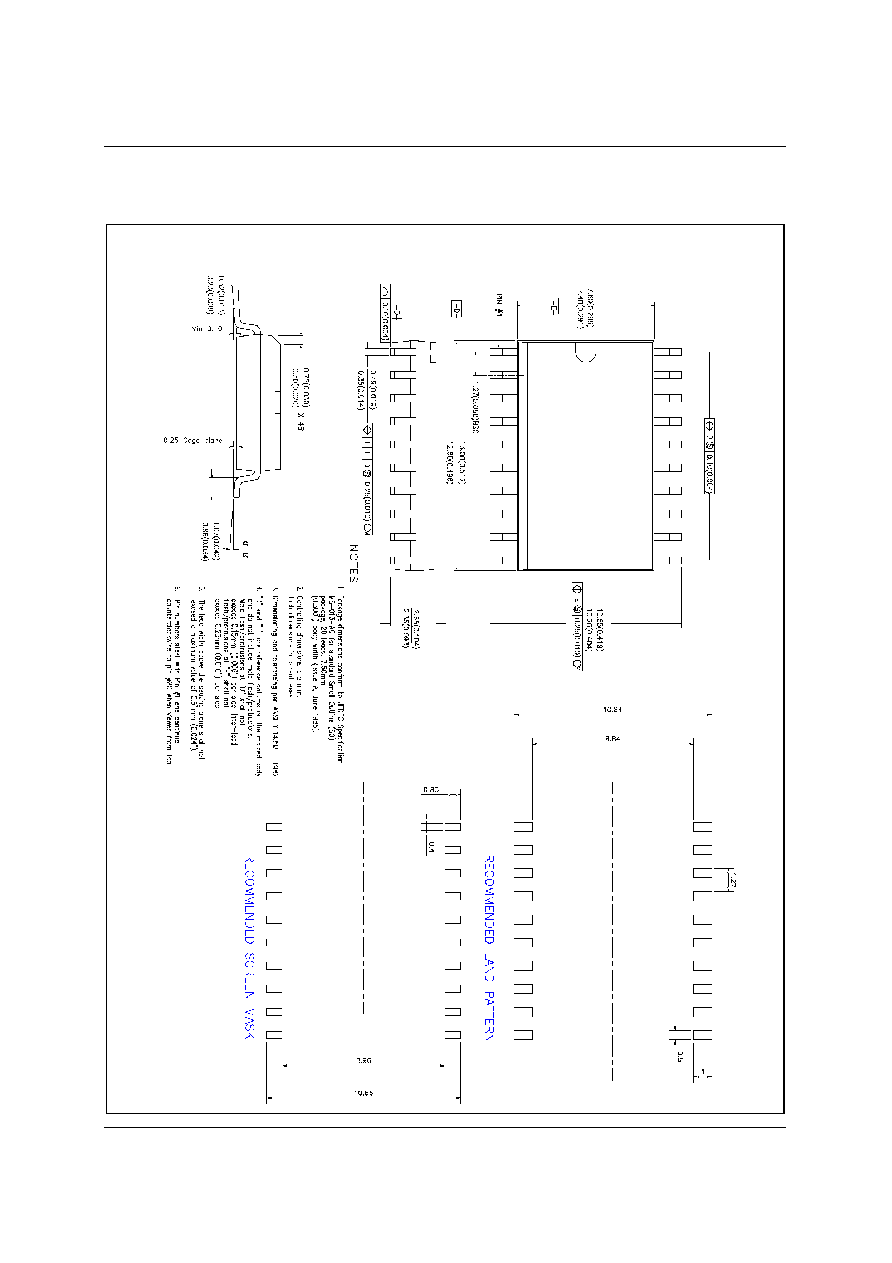
Mechanical Dimensions
Package
Dimensions in millimeters/inches
20SOP

FAN7040
11
Ordering Information
Device
Package
Operating Temperature
Remarks
FAN7040M
20SOP
-40
∞C ~ +85∞C
Tube
FAN7040MX
Tape & Reel

FAN7040
6/30/04 0.0m 001
Stock#DSxxxxxxxx
2004 Fairchild Semiconductor Corporation
LIFE SUPPORT POLICY
FAIRCHILD'S PRODUCTS ARE NOT AUTHORIZED FOR USE AS CRITICAL COMPONENTS IN LIFE SUPPORT DEVICES
OR SYSTEMS WITHOUT THE EXPRESS WRITTEN APPROVAL OF THE PRESIDENT OF FAIRCHILD SEMICONDUCTOR
CORPORATION. As used herein:
1. Life support devices or systems are devices or systems
which, (a) are intended for surgical implant into the body,
or (b) support or sustain life, and (c) whose failure to
perform when properly used in accordance with
instructions for use provided in the labeling, can be
reasonably expected to result in a significant injury of the
user.
2. A critical component in any component of a life support
device or system whose failure to perform can be
reasonably expected to cause the failure of the life support
device or system, or to affect its safety or effectiveness.
www.fairchildsemi.com
DISCLAIMER
FAIRCHILD SEMICONDUCTOR RESERVES THE RIGHT TO MAKE CHANGES WITHOUT FURTHER NOTICE TO ANY
PRODUCTS HEREIN TO IMPROVE RELIABILITY, FUNCTION OR DESIGN. FAIRCHILD DOES NOT ASSUME ANY
LIABILITY ARISING OUT OF THE APPLICATION OR USE OF ANY PRODUCT OR CIRCUIT DESCRIBED HEREIN; NEITHER
DOES IT CONVEY ANY LICENSE UNDER ITS PATENT RIGHTS, NOR THE RIGHTS OF OTHERS.