 | –≠–ª–µ–∫—Ç—Ä–æ–Ω–Ω—ã–π –∫–æ–º–ø–æ–Ω–µ–Ω—Ç: FAN7300G | –°–∫–∞—á–∞—Ç—å:  PDF PDF  ZIP ZIP |
©2003 Fairchild Semiconductor Corporation
www.fairchildsemi.com
Rev. 1.0.0
Features
∑ High Efficiency Single Stage Power Conversion
∑ Wide Input Voltage Range 6V to 25V
∑ Back Light Lamp Ballast and Soft Dimming
∑ Few External Components
∑ Precision Voltage Reference Trimmed to 2%
∑ Soft Start
∑ PWM and PFM Control
∑ Analog, Burst and Mixed Dimming Function
∑ Allows All N-Channel MOSFET Drive
∑ Double Pulse Suppression Logic
∑ Open Lamp Detection
∑ Output Short Circuit Protection
∑ Open Lamp Regulation
∑ 20 Pin SSOP
Description
The FAN7300 provides all the control functions for a
series parallel resonant converter and also contains a pulse
width modulation (PWM) controller to develop a supply
voltage. Typical operating frequency range is between
30kHz and 100kHz depending on the CCFL and the
transformer's characteristics.
20-SSOP
FAN7300
FAN7300
FAN7300
FAN7300
LCD Back Light Inverter Drive IC
LCD Back Light Inverter Drive IC
LCD Back Light Inverter Drive IC
LCD Back Light Inverter Drive IC

FAN7300
2
Internal Block Diagram
Dimming control and Mode Selection
Analog
Burst
Mixed
50K
50K
DIM
-
+
+
OLR
-
+
S_S
EA_OUT
Va
+
-
Vm2
Vmo
Multiplier
Gain
Buffer
Vm1
K
Low side
gate driver
Clock
Main Control
Oscillator
R
S
-
+
Q
Q
max. 1.75V
min. 0.25V
UVLO
-
+
Vcc
Internal
Bias
1.5Vref
Vz
5.4V
ENA
8V
OUT_L
GND
CPUMP
Ct
Rt
-
+
-
+
-
+
-
+
OLP
SCP
R
S
Q
-
+
BCt
Vb
Va
Current
Generator
E/A
Controller
Error Amp.
COMP3
COMP1
COMP2
COMP4
COMP5
COMP6
COMP7
3V
1.5V
1.5V
V3
3V
3V
1.5V
3.7V
Vz
2uA
EA_IN
VS
OUT_H
DIM_MODE
VZ
3.7V
max. 1.75V
min. 0.25V
High side
gate driver
Vz
8uA
V3
3V

FAN7300
3
Pin Assignments
Pin Definitions
No
Name
Function Description
No
Name
Function Description
1
OLP
Open Lamp Protection
11
OUT_H
High Side Gate Drive Output
2
Rt
Timing Resistor
12
CPUMP
Charge Pump
3
Ct
Timing Capacitor
13
VZ
Zener Voltage
4
BCt
Burst Dimming Timing Capacitor
14
OLR
Open Lamp Regulation
5
S_S
Soft Start
15
SCP
Short Circuit Protection
6
ENA
Enable Input
16
EA_IN
Error Amplifier Input
7
VS
Voltage Sensing
17
EA_OUT
Error Amplifier Output
8
VCC
Supply Voltage
18
DIM
Dimming Input
9
GND
Ground
19
DIM_MODE
Dimming Mode Selection
10
OUT_L
Low Side Gate Drive Output
20
V3
3V Reference Voltage
FAN7300
20
19
18
17
16
15
14
13
12
11
10
9
8
7
6
5
4
3
2
1
OLP
Rt
Ct
BCt
SCP
ENA
VS
VCC
GND
OUT_L
V3
DI
M
_
MO
D
E
DIM
EA_
OU
T
EA_IN
OLR
VZ
CP
UM
P
OUT
_
H
S_S
FAN7300
4
Absolute Maximum Ratings
Vcc=10V, for typical values Ta=25
∞
C, for min/max values Ta is the operating ambient temperature range with
-25
∞
C
Ta
85
∞
C and 6V
Vcc
25V, unless otherwise specified.
Note:
1. Thermal resistance test board
Size: 76.2mm * 114.3mm * 1.6mm(1S0P)
JEDEC standard: JESD51-3, JESD51-7
2. Assume no ambient airflow
Characteristics
Symbol
Value
Unit
Supply Voltage
V
CC
6 ~ 25
V
Operating Temperature Range
Topr
-25 ~ 85
∞
C
Storage Temperature Range
Tstg
-65 ~ 150
∞
C
Thermal Resistance Junction-Air (Note1,2)
R
JA
112
∞
C/W
Power Dissipation
Pd
1.1
W

FAN7300
5
Electrical Characteristics
Vcc=10V, for typical values Ta=25
∞
C, for min/max values Ta is the operating ambient temperature range with
-25
∞
C
Ta
85
∞
C and 6V
Vcc
25V, unless otherwise specified.
Characteristics
Symbol
Test Condition
Min.
Typ.
Max.
Unit
REFERENCE SECTION
Reference Voltage
Vref
-
1.46
1.5
1.54
V
Line Regulation
Vref
8
V
CC
20V
-
2
25
mV
3V Regulation Voltage
V3
-
2.86
2.96
3.06
V
OSCILLATOR SECTION(MAIN)
Oscillation Frequency
fosc
Ct = 330pF, Rt = 14k
75
95
115
kHz
CT High Voltage
Vcth
-
-
1.75
-
V
CT Low Voltage
Vbct1
-
-
0.25
-
V
OSCILLATOR SECTION(BURST)
Oscillation Frequency
fosc
Ctb = 180nF
125
170
205
Hz
BCT High Voltage
Vbcth
-
-
1.75
-
V
BCT Low Voltage
Vbct1
-
-
0.25
-
V
ERROR AMP SECTION
Feedback Output High Voltage
Veh
EA_IN = 0V
3.2
3.7
4.2
V
Output Sink Current
lsin
EA_OUT = 2.2V
-
-
-1
mA
Output Source Current
lsur
EA_OUT = 2.2V
1
-
-
mA
Feedback High Voltage On Burst Dimming
Vfbh
R(EA_IN) = 50k
Va+0.1 Va+0.4
Va+0.7
V
MULTIPLIER SECTION
Multiplier Input Voltage High
Vmih
-
1.4
1.6
1.8
V
Multiplier Gain
K
-
-
0.85
-
1/V
SOFT START SECTION
Soft Start Current
I
SS
S_S=2V
5
8.3
11.6
uA
Soft Start Clamping Voltage
Vssh
-
3
3.7
4.4
V
PROTECTION SECTION
Open Lamp Protection Voltage
Vpr
-
2.5
3
3.5
V
Short Circuit Protection Voltage
Vsc
-
2.5
3
3.5
V
Open Lamp Regulation
Vor
-
2.5
3
3.5
V

FAN7300
6
Electrical Characteristics
(Continued)
Vcc=10V, for typical values Ta=25
∞
C, for min/max values Ta is the operating ambient temperature range with
-25
∞
C
Ta
85
∞
C and 6V
Vcc
25V, unless otherwise specified.
Characteristics
Symbol
Test Condition
Min.
Typ.
Max.
Unit
DIMMING SECTION
Analog Dimming Range
Vaal
Dim_Mode > 2V, Dim = 0
-0.5
0
0.5
V
Vaah
Dim_Mode > 2V, Dim = 3V
2.5
3
3.5
V
Vba
Dim_Mode > 2V
-
3
-
V
Burst Dimming Range
Vbbl
Dim_Mode < 1V, Dim = 0
-0.5
0
0.5
V
Vbbh
Dim_Mode < 1V, Dim = 3V
2.1
2.5
2.9
V
Vab
Dim_Mode < 1V
2.45
2.85
3.25
V
Mixed Dimming Range
Vaml
Dim_Mode = 1.5V, Dim = 0
1.2
1.4
1.6
V
Vamh
Dim_Mode = 1.5V, Dim = 3V
2.5
3
3.5
V
Vbml
Dim_Mode = 1.5V, Dim = 0
-0.5
0
0.5
V
Vbmh
Dim_Mode = 1.5V, Dim = 3V
2.5
3
3.5
V
Analog Dimming Select Voltage
Vsa
-
1.5
2
2.5
V
Burst Dimming Select Voltage
Vsb
-
0.7
1
1.3
V
Mixed Dimming Select Voltage
Vsm
-
1.3
1.5
1.7
V
UNDER VOLTAGE LOCK OUT SECTION
Start Threshold Voltage
Vth
-
4.8
5.4
6.0
V
Start Up Current
Ist
V
CC
= 4.5V
-
150
250
uA
Operating Supply Current
Iop
V
CC
= 10V
-
8.5
11
mA
Stand-by Current
Isb
V
CC
= 12V
-
80
150
uA
ON/OFF SECTION
On State Input Voltage
Von
-
0.7
-
-
V
OUTPUT SECTION
Output High Voltage
Voh
V
CC
= 7V
5
-
-
V
Output Low Voltage
Vol
V
CC
= 7V
-
-
0.2
V
Output Voltage With UVLO Activated
Vuv
V
CC
= 4.5V
-
-
0.9
V
Output High Clamping Voltage
Vohc
V
CC
= 20V
11
13.5
16
V
Rising Time
Tr
V
CC
= 7V
-
100
200
ns
Falling Time
Tf
V
CC
= 7V
-
50
200
ns

FAN7300
7
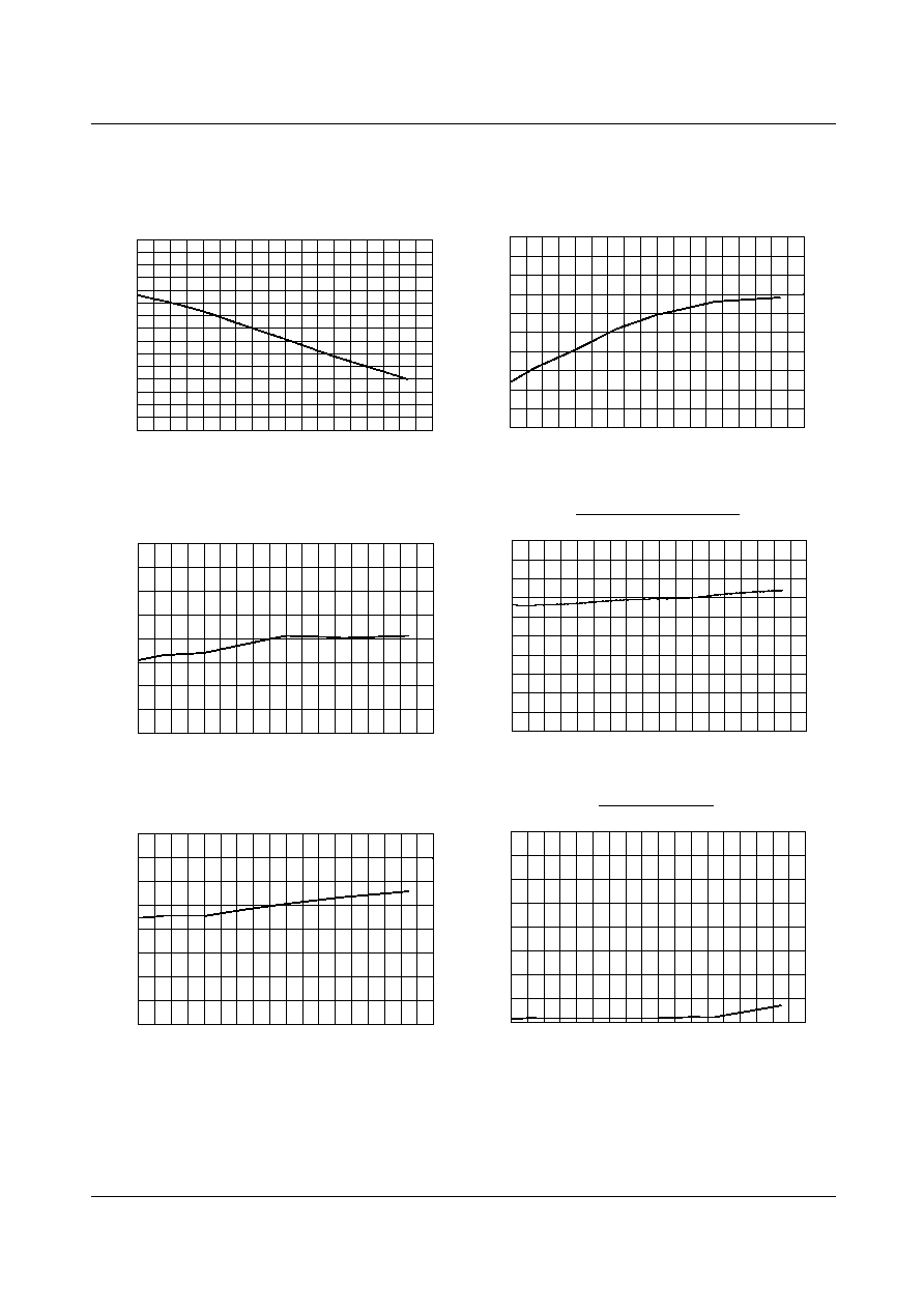
Typical Performance Characteristics
0
5
10
15
20
25
0
3
6
9
12
Supply Current vs Supply Voltage
ICC [mA]
VCC [V]
-40
-20
0
20
40
60
80
100
120
140
4.8
5.0
5.2
5.4
5.6
Startup Voltage
Vth [V
]
TEMP [? ]
-40
-20
0
20
40
60
80
100
120
140
0
20
40
60
80
Start Up Current
Is
t
[u
A
]
TEMP [? ]
-40
-20
0
20
40
60
80
100
120
140
2.90
2.92
2.94
2.96
2.98
3.00
3V Reference Voltage
V3 [
V
]
TEMP [? ]
-40
-20
0
20
40
60
80
100
120
140
0
2
4
6
8
10
12
Operating Supply Current
I
op [
m
A]
TEMP [? ]
-40
-20
0
20
40
60
80
100
120
140
0
20
40
60
80
100
120
Standby Current
Is
b
[u
A
]
TEMP [? ]
Figure 1. Supply Current vs. Supply Voltage
Figure 2. Start up Voltage
Figure 3. Start up Current
Figure 4. 3V Reference Voltge
Figure 5. Operating Supply Current
Figure 6. Stand by Current
Temp [
∞
C]
Temp [
∞
C]
Temp [
∞
C]
Temp [
∞
C]
Temp [
∞
C]
FAN7300
8
Typical Performance Characteristics
(Continued)
-40
-20
0
20
40
60
80
100
120
140
0.6
0.8
1.0
1.2
1.4
1.6
1.8
2.0
On State Input Voltage
Von [
V
]
TEMP [? ]
-40
-20
0
20
40
60
80
100
120
140
5
6
7
8
9
10
Soft Start Current
I
ss [
u
A
]
TEMP [? ]
-40
-20
0
20
40
60
80
100
120
140
80
90
100
110
Ocillastion Frequency (main)
Fosc [
K
hz
]
TEMP [? ]
-40
-20
0
20
40
60
80
100
120
140
100
120
140
160
180
200
Oscillator Frequency (Burst)
F
b
os
c
[
K
hz
]
TEMP [? ]
-40
-20
0
20
40
60
80
100
120
140
5.0
5.5
6.0
6.5
7.0
Output High Voltage
Voh [
V
]
TEMP [? ]
-40
-20
0
20
40
60
80
100
120
140
0.00
0.05
0.10
0.15
0.20
Output Low Voltage
Vo
l
[
V
]
TEMP [? ]
Figure 7. On State Input Voltage
Figure 8. Soft Start Current
Figure 9. Ocillastion Frequency (main)
Figure 10. Ocillastion Frequency (Burst)
Figure 11. Output High Voltage
Figure 12. Output Low Voltage
Temp [
∞
C]
Temp [
∞
C]
Temp [
∞
C]
Temp [
∞
C]
Temp [
∞
C]
Temp [
∞
C]

FAN7300
9
Typical Performance Characteristics
(Continued)
-40
-20
0
20
40
60
80
100
120
140
12.0
12.5
13.0
13.5
14.0
14.5
15.0
Output High Clamping Voltage
Vohc [
V
]
TEMP [? ]
-40
-20
0
20
40
60
80
100
120
140
0.0
0.1
0.2
0.3
0.4
0.5
0.6
0.7
Output Voltage with UVLO Activated
Vuv [
V
]
TEMP [? ]
-40
-20
0
20
40
60
80
100
120
140
2.6
2.8
3.0
3.2
3.4
Open Lamp Protection Voltage
Vp
r
[
V
]
TEMP [? ]
-40
-20
0
20
40
60
80
100
120
140
2.6
2.8
3.0
3.2
3.4
Short Circuit Protection Voltage
Vsc [
V
]
TEMP [? ]
-40
-20
0
20
40
60
80
100
120
140
2.50
2.75
3.00
3.25
3.50
Open Lamp Regulation Voltage
Vo
r
[
V
]
TEMP [? ]
-40
-20
0
20
40
60
80
100
120
140
3.0
3.2
3.4
3.6
3.8
4.0
4.2
4.4
Error Amp. Output High Voltage
Veh [
V
]
TEMP [? ]
Figure 13. Output High Clamping Voltage
Figure 14. Output Voltage With UVLO Activated
Figure 15. Open Lamp Protection Voltage
Figure 17. Open Lamp Regulation Voltage
Figure 16. Short Circuit Protection Voltage
Figure 18. Error Amp Output High Voltage
Temp [
∞
C]
Temp [
∞
C]
Temp [
∞
C]
Temp [
∞
C]
Temp [
∞
C]
Temp [
∞
C]

FAN7300
10
Typical Performance Characteristics
(Continued)
-40
-20
0
20
40
60
80
100
120
140
-6.0
-5.5
-5.0
-4.5
-4.0
-3.5
-3.0
-2.5
-2.0
Output Sink Current
Is
i
n
[
m
A
]
TEMP [? ]
-40
-20
0
20
40
60
80
100
120
140
2.0
2.5
3.0
3.5
4.0
4.5
5.0
5.5
6.0
Output Source Current
Is
u
r
[
m
A
]
TEMP [? ]
Figure 19. Output Sink Current
Figure 20. Output Source Current
Temp [
∞
C]
Temp [
∞
C]

FAN7300
11
Mechanical Dimensions
Package
Dimensions in millimeters
20-SSOP

FAN7300
4/22/03 0.0m 001
Stock#DSxxxxxxxx
2002 Fairchild Semiconductor Corporation
LIFE SUPPORT POLICY
FAIRCHILD'S PRODUCTS ARE NOT AUTHORIZED FOR USE AS CRITICAL COMPONENTS IN LIFE SUPPORT DEVICES
OR SYSTEMS WITHOUT THE EXPRESS WRITTEN APPROVAL OF THE PRESIDENT OF FAIRCHILD SEMICONDUCTOR
CORPORATION. As used herein:
1. Life support devices or systems are devices or systems
which, (a) are intended for surgical implant into the body,
or (b) support or sustain life, and (c) whose failure to
perform when properly used in accordance with
instructions for use provided in the labeling, can be
reasonably expected to result in a significant injury of the
user.
2. A critical component in any component of a life support
device or system whose failure to perform can be
reasonably expected to cause the failure of the life support
device or system, or to affect its safety or effectiveness.
www.fairchildsemi.com
DISCLAIMER
FAIRCHILD SEMICONDUCTOR RESERVES THE RIGHT TO MAKE CHANGES WITHOUT FURTHER NOTICE TO ANY
PRODUCTS HEREIN TO IMPROVE RELIABILITY, FUNCTION OR DESIGN. FAIRCHILD DOES NOT ASSUME ANY
LIABILITY ARISING OUT OF THE APPLICATION OR USE OF ANY PRODUCT OR CIRCUIT DESCRIBED HEREIN; NEITHER
DOES IT CONVEY ANY LICENSE UNDER ITS PATENT RIGHTS, NOR THE RIGHTS OF OTHERS.
Ordering Information
Product number
Package
Operating Temperature
FAN7300G
20-SSOP
-25
∞
C ~ 85
∞
C