 | –≠–ª–µ–∫—Ç—Ä–æ–Ω–Ω—ã–π –∫–æ–º–ø–æ–Ω–µ–Ω—Ç: FAN7380MX | –°–∫–∞—á–∞—Ç—å:  PDF PDF  ZIP ZIP |

©2005 Fairchild Semiconductor Corporation
www.fairchildsemi.com
Rev. 1.0.0
Features
∑ Floating Channel Designed For Bootstrapping Operation
To +600V
∑ Typically 90mA/180mA Sourcing/Sinking Current
Driving Capability For Both Channels
∑ Common-Mode dv/dt Noise Canceling Circuit
∑ Extended Allowable Negative VS Swing To -9.8V For
Signal Propagation @ VCC=VBS=15V
∑ VCC & VBS Supply Range From 10V To 20V
∑ UVLO Functions For Both Channels
∑ TTL Compatible Input Logic Threshold Levels
∑ Matched Propagation Delay Below 50nsec
∑ Built-in 100nsec Dead-Time Control Function
∑ Output In-Phase With Input
Typical Applications
∑ Fluorescent Lamp Ballast
∑ Compact Fluorescent Lamp Ballast
Description
The FAN7380 is a monolithic half-bridge gate driver IC for
MOSFETs and IGBTs, which operate up to +600V. Fair-
child's high voltage process and common-mode noise can-
celing technique give stable operation of high-side driver
under high dv/dt noise circumstances. Advanced level shift
circuit allows high-side gate driver operation up to VS=-
9.8V(typ.) for VBS=15V. The input logic level is compatible
with standard TTL series logic gates. The internal shoot-
through protection circuit provides 100nsec dead-time to
prevent output switching devices from both conduction dur-
ing transition periods. UVLO circuits for both channels pre-
vent malfunction when VCC and VBS are lower than the
specified threshold voltage. Output drivers typically source/
sink 90mA/180mA, respectively, which is suitable for the
applications such as fluorescent/compact fluorescent lamp
ballast applications and the systems that require low di/dt
noise.
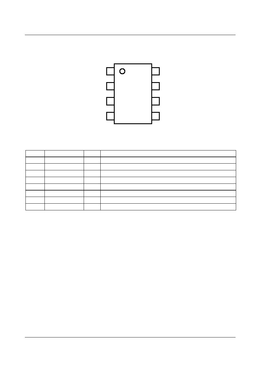
8SOIC
1
FAN7380
Half-Bridge Gate Driver
(SOURCING/SINKING : 90mA/180mA)
Internal Block Diagram
HO
LO
COM
V
CC
HIN
LIN
5
6
7
V
S
V
B
DELAY
SHOOT-TROU
G
H
P
R
EV
EN
TI
ON
LEVEL
SHIFTER
NOISE
CANCELLER
1
4
2
8
3
PULSE
GENERATION
R
S
R
Q
UVLO
UVLO
DRI
VER
DRIVER
LOW-SIDE DRIVER
HIGH-SIDE DRIVER
FAN7380
2
Pin Assignments
Pin Descriptions
Pin No
Symbol
I/O
Description
1
LIN
Logic Input for Low Side Gate Driver Output
2
HIN
Logic Input for High Side Gate Driver Output
3
VCC
Low Side Supply Voltage
4
COM
Logic Ground and Low Side Driver Return
5
LO
Low Side Driver Output
6
VS
High Voltage Floating Supply Return
7
HO
High Side Driver Output
8
VB
High Side Floating Supply
HIN
LIN
V
CC
COM
LO
V
S
HO
V
B
1
2
3
4
8
7
6
5
F
A
N
7
380
FAN7380
3
Absolute Maximum Ratings
Note : Absolute maximum ratings indicate sustained limits beyond which damage to the device may occur. All voltage parameters
are absolute voltage referenced to COM, all currents are defined positive into any lead.
Recommended Operating Ratings
ESD Level
Parameter
Symbol
Min.
Typ.
Max.
Unit
High side offset Voltage
V
S
V
B
-25
-
V
B
+0.3
V
High side floating supply voltage
V
B
-0.3
625
High side floating output voltage
HO
V
HO
V
S
-0.3
V
B
+0.3
Low side and logic fixed supply
voltage
V
CC
-0.3
25
Low side output voltage LO
V
LO
-0.3
V
CC
+0.3
Logic input voltage(HIN, LIN)
V
IN
-0.3
V
CC
+0.3
Logic Ground
COM
V
CC
-25
V
CC
+0.3
Allowable offset voltage SLEW
RATE
dV
S
/dt
50
V/ns
Power Dissipation
P
D
0.625
W
Thermal resistance, junction to
ambient
Rthja
200
∞C/W
Junction Temperature
T
J
150
∞C
Storage Temperature
T
S
-50
150
∞C
Parameter
Symbol
Min.
Typ.
Max.
Unit
High side floating supply voltage
V
B
V
S
+10
-
V
S
+20
V
High side floating supply offset
voltage
V
S
6-VCC
600
High side(HO) output voltage
V
HO
V
S
V
B
Low side(LO) output voltage
V
LO
COM
V
CC
Logic input voltage(HIN, LIN)
V
IN
COM
V
CC
Low side supply voltage
V
CC
10
20
Ambient Temperature
T
A
-40
125
∞C
Parameter
PIns
Conditions
Level
Unit
Human Body Model(HBM)
HIN, LIN, VCC, COM, VB, HO
R=1.5k
, C=100pF
±1500
V
LO, VS
±1000
Machine Model(MM)
All Pins
C=200pF
±300
Charged Device Model(CDM)
All Pins
±500

FAN7380
4
Static Electrical Characteristics
(V
BIAS
(V
CC
, V
BS
)=15.0V, T
A
= 25
∞C, unless otherwise specified. The V
IN
, V
TH
and I
IN
parameters are referenced
to COM. The V
O
and I
O
parameters are referenced to COM and V
S
is applicable to HO and LO.)
Dynamic Electrical Characteristics
(V
BIAS
(V
CC
, V
BS
)=15.0V, V
S
=COM, C
L
=1000pF and T
A
= 25
∞C, unless otherwise specified.)
Parameter
Symbol
Conditions
Min.
Typ. Max.
Unit
VCC & VBS supply under voltage
positive going threshold
V
CCUV+
V
BSUV+
8.2
9.2
10.0
V
VCC & VBS supply under voltage
negative going threshold
V
CCUV-
V
BSUV-
7.6
8.7
9.6
VCC supply under voltage lockout
hysteresis
V
CCUVH
V
BSUVH
-
0.5
-
Offset supply leakage current
I
LK
V
B
=V
S
=600V
-
-
50
µA
Quiescent VBS supply current
I
QBS
V
IN
=0V or 5V
-
44
100
Quiescent VCC supply current
I
QCC
V
IN
=0V or 5V
-
70
180
Operating VBS supply current
I
PBS
fin=20kHz, rms value
-
-
600
µA
Operating VCC supply current
I
PCC
fin=20kHz, rms value
-
-
610
Logic "1" input voltage
V
IH
2.5
-
-
V
Logic "0" input voltage
V
IL
-
-
0.8
High level output voltage,
V
BIAS
-V
O
V
OH
I
O
=20mA
-
-
2.8
V
Low level output voltage, VO
V
OL
-
-
1.2
Logic "1" input bias current
I
IN+
V
IN
=5V
-
5
40
µA
Logic "0" input bias current
I
IN-
V
IN
=0V
-
1.0
2.0
Output high short circuit pulse
current
I
O+
V
O
=0V PW<=10us
60
90
-
mA
Output low short circuit pulsed
current
I
O-
130
180
-
Allowable negative V
S
pin voltage
for HIN signal propagation to HO
V
S
-
-9.8
-7
V
Parameter
Symbol
Conditions
Min.
Typ. Max.
Unit
Turn-on propagation delay
t
on
V
S
=0V
70
135
200
ns
Turn-off propagation delay
t
off
V
S
=0V or 600V
60
130
190
Turn-on rise time
t
r
160
230
290
Turn-off fall time
t
f
20
90
160
Dead time
DT
80
100
190
Delay matching, HS & LS turn-on/
off
MT
-
-
50

FAN7380
5
Typical Characteristics
Fig. 5 Turn-On Rising Time vs. Supply Voltage
Fig. 6 Turn-On Rising Time vs. Temperature
Fig. 1 Turn-On Propagation Delay vs. Supply Voltage
Fig. 2 Turn-On Propagation Delay vs. Temperature
Fig. 3 Turn-Off Propagation Delay vs. Supply Voltage
Fig. 4 Turn-Off Propagation Delay vs. Temperature
10
12
14
16
18
20
80
90
100
110
120
130
140
150
160
170
180
190
200
T
u
rn-On
Propagation D
e
l
a
y
[nsec
]
Supply Voltage [V]
High-Side
Low-Side
VCC=VBS
COM=0V
CL=1nF
Ta=25∞C
10
12
14
16
18
20
80
90
100
110
120
130
140
150
160
170
180
190
200
T
u
rn-On
Propagation D
e
l
a
y
[nsec
]
Supply Voltage [V]
High-Side
Low-Side
VCC=VBS
COM=0V
CL=1nF
Ta=25∞C
-40
-20
0
20
40
60
80
100
120
80
90
100
110
120
130
140
150
160
170
180
190
200
T
u
rn-O
n
Propagat
ion Delay
[
n
sec
]
Temperature [∞C]
High-Side
Low-Side
VCC=VBS=15V
COM=0V
CL=1nF
-40
-20
0
20
40
60
80
100
120
80
90
100
110
120
130
140
150
160
170
180
190
200
T
u
rn-O
n
Propagat
ion Delay
[
n
sec
]
Temperature [∞C]
High-Side
Low-Side
VCC=VBS=15V
COM=0V
CL=1nF
10
12
14
16
18
20
80
100
120
140
160
180
200
T
u
rn-
O
f
f
P
r
opa
g
a
ti
on
Del
a
y
[
n
sec
]
Supply Voltage [V]
High-Side
Low-Side
VCC=VBS
COM=0V
CL=1nF
Ta=25∞C
10
12
14
16
18
20
80
100
120
140
160
180
200
T
u
rn-
O
f
f
P
r
opa
g
a
ti
on
Del
a
y
[
n
sec
]
Supply Voltage [V]
High-Side
Low-Side
VCC=VBS
COM=0V
CL=1nF
Ta=25∞C
-40
-20
0
20
40
60
80
100
120
80
90
100
110
120
130
140
150
160
170
180
190
200
T
u
r
n
-
O
f
f
P
r
op
ag
at
i
o
n
De
l
a
y
[
n
se
c]
Temperature [∞C]
High-Side
Low-Side
VCC=VBS=15V
COM=0V
CL=1nF
-40
-20
0
20
40
60
80
100
120
80
90
100
110
120
130
140
150
160
170
180
190
200
T
u
r
n
-
O
f
f
P
r
op
ag
at
i
o
n
De
l
a
y
[
n
se
c]
Temperature [∞C]
High-Side
Low-Side
VCC=VBS=15V
COM=0V
CL=1nF
10
12
14
16
18
20
100
150
200
250
300
350
T
u
rn-On
R
i
s
i
ng
T
i
me
[n
se
c
]
Supply Voltage [V]
Low-Side
High-Side
VCC=VBS
COM=0V
CL=1nF
Ta=25∞C
10
12
14
16
18
20
100
150
200
250
300
350
T
u
rn-On
R
i
s
i
ng
T
i
me
[n
se
c
]
Supply Voltage [V]
Low-Side
High-Side
VCC=VBS
COM=0V
CL=1nF
Ta=25∞C
-40
-20
0
20
40
60
80
100
120
100
120
140
160
180
200
220
240
260
280
300
T
u
rn-O
n
Ri
s
i
ng
T
i
me
[nsec]
Temperature [∞C]
High-Side
Low-Side
VCC=VBS=15V
COM=0V
CL=1nF
-40
-20
0
20
40
60
80
100
120
100
120
140
160
180
200
220
240
260
280
300
T
u
rn-O
n
Ri
s
i
ng
T
i
me
[nsec]
Temperature [∞C]
High-Side
Low-Side
VCC=VBS=15V
COM=0V
CL=1nF