 | –≠–ª–µ–∫—Ç—Ä–æ–Ω–Ω—ã–π –∫–æ–º–ø–æ–Ω–µ–Ω—Ç: FAN7527 | –°–∫–∞—á–∞—Ç—å:  PDF PDF  ZIP ZIP |
©2002 Fairchild Semiconductor Corporation
www.fairchildsemi.com
Rev 1.0.1
Features
∑ Internal Start-up Timer
∑ Internal R/C Filter Eliminates the Need for an External
R/C Filter
∑ Very Precise Adjustable Output Over Voltage Protection
∑ Zero Current Detector
∑ One Quadrant Multiplier
∑ Trimmed 1.5% Internal Band Gap Reference
∑ Under Voltage Lockout with 3V of Hysteresis
∑ Totem Pole Output With High State Clamp
∑ Low Start-up and Operating Current
∑ 8-Pin DIP or 8-Pin SOP
Applications
∑ Electronic Ballast
∑ SMPS
Description
The FAN7527B provides simple and high performance
active power factor correction. The FAN7527B is optimized
for electronic ballasts and low power and high density power
supplies which require minimum board size, reduced
external components and low power dissipation. Because the
R/C filter is included in the current sense block, the external
R/C filter is not necessary. Special circuitry has also been
added to prevent no load runaway conditions. Regardless of
the supply voltage, the output drive clamping circuit limits
the overshoot of the power MOSFET gate drive. It greatly
enhances the system reliability.
FAN7527B
Power Factor Correction Controller
8-DIP
8-SOP
1
1
FAN7527B
2
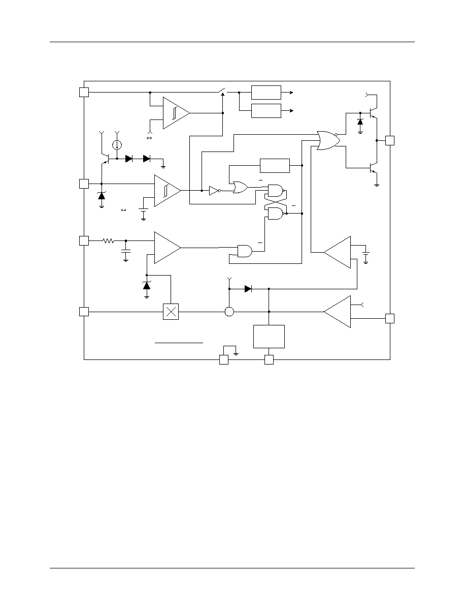
Internal Block Diagram
INV
1
2
Vea(-)
Error Amp
Vref
+
+
+
+
-
-
-
-
OVP
Current
Detector
Isovp=30uA
Idovp=40uA
+
+
+
+
-
-
-
-
Vref
Vm2
Vref~Vref+2.5V
2.25V
Static OVP
+
+
+
+
-
-
-
-
EA_OUT
6
GND
)
(
Vref
2
Vm
1
Vm
Vmo
K
-
-
-
-
=
=
=
=
Multiplier
+
+
+
+
-
-
-
-
Vm1
Vmo
0 ~ 3.8V
8pF
40k
+
+
+
+
-
-
-
-
+
+
+
+
-
-
-
-
2.5V Ref
Internal
Bias
Timer R
7
Vcc
5
4
3
8
Vcc
Idet
CS
MULT
OUT
Drive
Output
0.25V
Veao(L)=2.25V
R
Q
S
UVLO
7.2V
Zero Current
Detector
Current Sense
Comparator
1.8V
2V 1.5V
11.5V
8.5V
FAN7527B
3
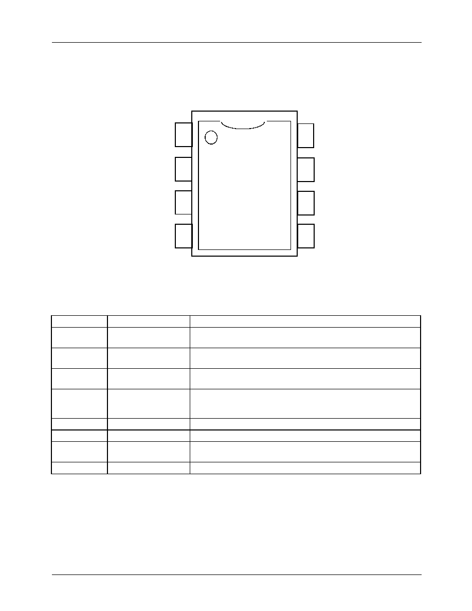
PIN Description
Pin Number
Pin Name
Pin Function Description
1
INV
Inverting input of the error amplifier. The output of the boost converter
should be resistively divided to 2.5V and connected to this pin.
2
EA_OUT
The output of the error amplifier. A feedback compensation network is
placed between this pin and the INV pin.
3
MULT
Input to the multiplier stage. The full-wave rectified AC voltage is
divided to less than 2V and is connected to this pin.
4
CS
Input of the PWM comparator. The MOSFET current is sensed by a
resistor and the resulting voltage is applied to this pin. An internal R/C
filter is included to reject any high frequency noise.
5
ldet
Zero current detection input.
6
GND
The ground potential of all the pins.
7
OUT
Gate driver output. The push pull output stage is able to drive the
Power MOSFET with peak current of 500mA.
8
Vcc
Supply voltage of driver and control circuits.
1
2
3
4
8
7
6
5
Vcc
OUT
MULT
CS
GND
ldet
EA_OUT
INV
(Top View)
FAN7527B
4
Absolute Maximum Ratings (Ta=25
∞
∞
∞
∞
C)
Temperature Characteristics (-25
∞
∞
∞
∞
C
Ta
125
∞
∞
∞
∞
C)
Characteristics
Symbol
Value
Unit
Supply Voltage
V
CC
30
V
Peak Drive Output Current
I
OH
,I
OL
±500
mA
Driver Output Clamping Diodes Vo > Vcc or Vo < -0.3V
lclamp
±10
mA
Detector Clamping Diodes
ldet
±10
mA
Error Amp, Multiplier and Comparator Input Voltages
Vin
-0.3 to 6
V
Operating Junction Temperature
Tj
150
∞
C
Operating Temperature Range
Topr
-25 to 125
∞
C
Storage Temperature Range
Tstg
-65 to 150
∞
C
Power Dissipation
Pd
0.8
W
Characteristics
Symbol
Min.
Typ.
Max.
Unit
Temperature Stability for Reference Voltage (V
ref
)
Vref
-
20
-
mV
Temperature Stability for Multiplier Gain (K)
K/
T
-
-0.2
-
%/
∞
C

FAN7527B
5
Electrical Characteristics
V
CC
= 14V, -25
∞
C
Ta
125
∞
C
,
unless otherwise stated.
Characteristics
Symbol
Test Condition
Min.
Typ.
Max.
Unit
< UNDER VOLTAGE LOCKOUT SECTION>
Start Threshold Voltage
V
th(st)
Vcc Increasing
10.5
11.5
12.5
V
UVLO Hysteresis
HY(st)
-
2
3
4
V
< SUPPLY CURRENT SECTION >
Start-up Supply Current
I
st
Vcc = Vth(st) -0.2V
10
60
100
uA
Operating Supply Current
I
cc
Output not switching
-
3
6
mA
Operating Current at OVP
I
cc(ovp)
Vinv = 3V
-
1.7
4
mA
Dynamic Operating Supply Current
I
dcc
50kHz, CI = 1nF
-
4
8
mA
< ERROR AMPLIFIER SECTION >
Voltage Feedback Input Threshold
V
ref
Iref = 0mA, Ta = 25
∞
C
2.465
2.5
2.535
V
-25
Ta
125
∞
C
2.44
2.5
2.56
V
Line Regulation
V
ref
1
14V
Vcc
25V
-
0.1
10
mV
Temperature Stability of Vref (Note1)
V
ref
3
-25
Ta
125
∞
C
-
20
-
mV
Input Bias Current
Ib
(ea)
-
-0.5
-
0.5
uA
Output Source Current
I
source
Vm2 = 4V
-2
-4
-
mA
Output Sink Current
Isink
Vm2 = 4V
2
4
-
mA
Output Upper Clamp Voltage (Note2)
Veao(H)
Isource = 0.1mA
-
6
-
V
Output Lower Clamp Voltage (Note3)
Veao(L)
Isink = 0.1mA
-
2.25
-
V
Large Signal Open Loop Gain (Note4)
G
v
-
60
80
-
dB
Power Supply Rejection Ratio (Note5)
PSRR
14V
Vcc
25V
60
80
-
dB
Unity Gain Bandwidth (Note6)
GBW
-
-
1
-
MHz
Slew Rate (Note7)
SR
-
-
0.6
-
V/us
< MULTIPLIER SECTION>
Input Bias Current (Pin3)
Ib
(m)
-
-0.5
-
0.5
uA
M1 Input Voltage Range (Pin3)
V
m
1
-
0
-
3.8
V
M2 Input Voltage Range (Pin2)
V
m
2
-
Vref
-
Vref+2.5
V
Multiplier Gain (Note8)
K
Vm1 = 1V, Vm2 = 3.5V
0.36
0.44
0.52
1/V
Maximum Multiplier Output Voltage
Vomax(m) Vinv =0V, Vm1 = 4V
1.65
1.8
1.95
V
Temperature Stability of K (Note9)
K/
T
-25
Ta
125
∞
C
-
-0.2
-
%/
∞
C