 | –≠–ª–µ–∫—Ç—Ä–æ–Ω–Ω—ã–π –∫–æ–º–ø–æ–Ω–µ–Ω—Ç: FAN7530N | –°–∫–∞—á–∞—Ç—å:  PDF PDF  ZIP ZIP |
October 2006
F
AN7530 Critical Conduct
ion Mode PFC Controller
© 2006 Fairchild Semiconductor Corporation
www.fairchildsemi.com
FAN7530 Rev. 1.0.0
FAN7530
Critical Conduction Mode PFC Controller
Features
Low Total Harmonic Distortion (THD)
Precise Adjustable Output Over-Voltage Protection
Open-Feedback Protection and Disable Function
Zero Current Detector
150µs Internal Start-up Timer
MOSFET Over-Current Protection
Under-Voltage Lockout with 3.5V Hysteresis
Low Start-up (40µA) and Operating Current (1.5mA)
Totem Pole Output with High State Clamp
+500/-800mA Peak Gate Drive Current
8-Pin DIP or 8-Pin SOP
Applications
Adapter
Ballast
LCD TV, CRT TV
SMPS
Related Application Notes
AN-6027 - Design of Power Factor Correction Circuit
Using FAN7530
Description
The FAN7530 is an active power factor correction (PFC)
controller for boost PFC applications that operates in crit-
ical conduction mode (CRM). It uses the voltage mode
PWM that compares an internal ramp signal with the
error amplifier output to generate MOSFET turn-off sig-
nal. Since the voltage mode CRM PFC controller does
not need rectified AC line voltage information, it saves
the power loss of the input voltage sensing network nec-
essary for the current mode CRM PFC controller.
FAN7530 provides many protection functions, such as
over voltage protection, open-feedback protection, over-
current protection, and under-voltage lockout protection.
The FAN7530 can be disabled if the INV pin voltage is
lower than 0.45V and the operating current decreases to
65µA. Using a new variable on-time control method,
THD is lower than the conventional CRM boost PFC ICs.
Ordering Information
Part Number
Operating Temp.
Range
Pb-Free
Package Packing
Method
Marking
Code
FAN7530N
-40
∞C to +125∞C
Yes
8-DIP
Rail
FAN7530
FAN7530M
-40
∞C to +125∞C
Yes
8-SOP
Rail
FAN7530
FAN7530MX
-40
∞C to +125∞C
Yes
8-SOP
Tape & Reel
FAN7530
F
AN7530 Critical Conducti
on Mode PFC Controller
© 2006 Fairchild Semiconductor Corporation
www.fairchildsemi.com
FAN7530 Rev. 1.0.0
2
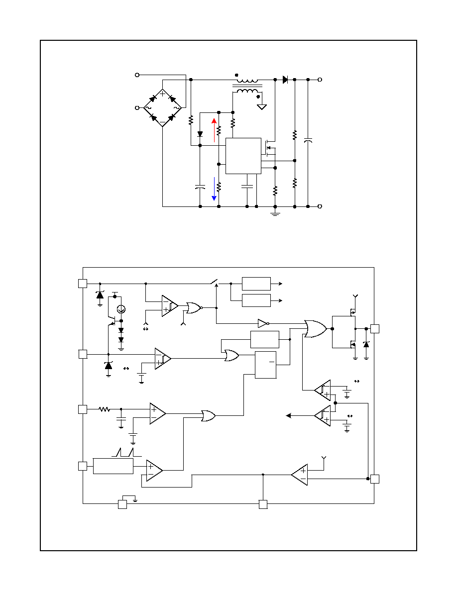
Typical Application Diagrams
Figure 1. Typical Boost PFC Application
Internal Block Diagram
Figure 2. Functional Block Diagram of FAN7530
GND
ZCD
INV
V
CC
AC
IN
V
O
COMP
FAN7530
CS
MOT
R1
R2
L
D
N
AUX
V
AUX
R
ZCD
I2
I1
C
O
FAN7530 Rev. 00
INV
Error
Amplifier
Vref
OVP
COMP
8pF
40k
2.5V
Ref
Internal
Bias
150ms
Timer
V
CC
ZCD
CS
UVLO
6.5V
12V 8.5V
2.675V
2.5V
Current Protection
Comparator
1V Offset
MOT
GND
Sawtooth
Generator
Zero Current
Detector
R
S
Q
2
6
4
5
3
1
8
Vref
Gm
0.8V
Disable
0.45V 0.35V
Disable
1.5V
1.4V
7
V
CC
OUT
Drive
Output
Ramp
Signal
1V~5V
Range
13V
FAN7530 Rev. 00
F
AN7530 Critical Conducti
on Mode PFC Controller
© 2006 Fairchild Semiconductor Corporation
www.fairchildsemi.com
FAN7530 Rev. 1.0.0
3
Pin Assignments
Figure 3. Pin Configuration (Top View)
Pin Definitions
Pin #
Name
Description
1
INV
This pin is the inverting input of the error amplifier. The output voltage of the boost PFC
converter should resistively divided to 2.5V.
2
MOT
This pin is used to set the slope of the internal ramp. The voltage of this pin is main-
tained at 2.9V. If a resistor is connected between this pin and GND, current flows out of
the pin and the slope of the internal ramp is proportional to this current.
3
COMP
This pin is the output of the transconductance error amplifier. Components for the out-
put voltage compensation should be connected between this pin and GND.
4
CS
This pin is the input of the over-current protection comparator. The MOSFET current is
sensed using a sensing resistor and the resulting voltage is applied to this pin. An
internal RC filter is included to filter switching noise.
5
ZCD
This pin is the input of the zero current detection block. If the voltage of this pin goes
higher than 1.5V, then goes lower than 1.4V, the MOSFET is turned on.
6
GND
This pin is used for the ground potential of all the pins. For proper operation, the signal
ground and the power ground should be separated.
7
OUT
This pin is the gate drive output. The peak sourcing and sinking current levels are
+500mA and -800mA respectively. For proper operation, the stray inductance in the
gate driving path must be minimized.
8
Vcc
This pin is the IC supply pin. IC current and MOSFET drive current are supplied using
this pin.
F A N 7 5 3 0
6
5
8
7
V
CC
OUT
GND
ZCD
1
2
3
4
COMP
CS
MOT
INV
Y W W
FAN7530 Rev. 00

F
AN7530 Critical Conducti
on Mode PFC Controller
© 2006 Fairchild Semiconductor Corporation
www.fairchildsemi.com
FAN7530 Rev. 1.0.0
4
Absolute Maximum Ratings
The "Absolute Maximum Ratings" are those values beyond which the safety of the device cannot be guaranteed. The
device should not be operated at these limits. The parametric values defined in the Electrical Characteristics tables
are not guaranteed at the absolute maximum ratings. T
A
=25∞C, unless otherwise specified.
Thermal Impedance
(1)
Note:
1. Regarding the test environment and PCB type, please refer to JESD51-2 and JESD51-10.
Symbol
Parameter
Value
Unit
V
CC
Supply Voltage
V
Z
V
I
OH
, I
OL
Peak Drive Output Current
+500/-800
mA
I
clamp
Driver Output Clamping Diodes V
O
>V
CC
or V
O
<-0.3V
±10
mA
I
det
Detector Clamping Diodes
±10
mA
V
IN
Error Amplifier, MOT, CS Input Voltages
-0.3 to 6
V
T
J
Operating Junction Temperature
150
∞C
T
A
Operating Temperature Range
-40 to 125
∞C
T
STG
Storage Temperature Range
-65 to 150
∞C
V
ESD_HBM
ESD Capability, Human Body Model
2.0
kV
V
ESD_MM
ESD Capability, Machine Model
300
V
V
ESD_CDM
ESD Capability, Charged Device Model
500
V
Symbol
Parameter
Value
Unit
JA
Thermal Resistance, Junction-to-Ambient
8-DIP
110
∞C/W
8-SOP
150
∞C/W

F
AN7530 Critical Conducti
on Mode PFC Controller
© 2006 Fairchild Semiconductor Corporation
www.fairchildsemi.com
FAN7530 Rev. 1.0.0
5
Electrical Characteristics
V
CC
= 14V and T
A
= -40∞C~125∞C unless otherwise specified.
Note:
2. These parameters, although guaranteed by design, are not tested in production.
Symbol Parameter
Condition
Min.
Typ.
Max.
Unit
UNDER-VOLTAGE LOCKOUT SECTION
V
th(start)
Start Threshold Voltage
V
CC
increasing
11
12
13
V
V
th(stop)
Stop Threshold Voltage
V
CC
decreasing
7.5
8.5
9.5
V
HY
(uvlo)
UVLO Hysteresis
3.0
3.5
4.0
V
V
Z
Zener Voltage
I
CC
= 20mA
22
V
SUPPLY CURRENT SECTION
I
st
Start-up Supply Current
V
CC
= V
th(start)
- 0.2V
40
70
µA
I
CC
Operating Supply Current
Output no switching
1.5
3.0
mA
I
dcc
Dynamic Operating Supply Current
50kHz, C
L
=1nF
2.5
4.0
mA
I
CC(dis)
Operating Current at Disable
V
inv
= 0V
20
65
95
µA
ERROR AMPLIFIER SECTION
V
ref1
Voltage Feedback Input Threshold1
T
A
= 25
∞C
2.465
2.500
2.535
V
V
ref1
Line Regulation
V
CC
= 14V ~ 20V
0.1
10.0
mV
V
ref2
Temperature Stability of V
ref1
(2)
20
mV
I
b(ea)
Input Bias Current
V
inv
= 1V ~ 4V
-0.5
0.5
µA
I
source
Output Source Current
V
inv
= V
ref1
- 0.1V
-12
µA
I
sink
Output Sink Current
V
inv
= V
ref1
+ 0.1V
12
µA
V
eao(H)
Output Upper Clamp Voltage
V
inv
= V
ref1
- 0.1V
5.4
6.0
6.6
V
V
eao(Z)
Zero Duty Cycle Output Voltage
0.9
1.0
1.1
V
g
m
Transconductance
(2)
90
115
140
µmho
MAXIMUM ON-TIME SECTION
V
mot
Maximum On-Time Voltage
R
mot
= 40.5k
2.784
2.900
3.016
V
t
on(max)
Maximum On-Time Programming
R
mot
= 40.5k
, T
A
= 25
∞C
19
24
29
µsec
CURRENT SENSE SECTION
V
CS(limit)
Current Sense Input Threshold
Voltage Limit
0.7
0.8
0.9
V
I
b(cs)
Input Bias Current
V
CS
= 0V ~ 1V
-1.0
-0.1
1.0
µA
t
d(cs)
Current Sense Delay to Output
(2)
dV/dt = 1V/100ns,
from 0V to 5V
350
500
nsec

F
AN7530 Critical Conducti
on Mode PFC Controller
© 2006 Fairchild Semiconductor Corporation
www.fairchildsemi.com
FAN7530 Rev. 1.0.0
6
Electrical Characteristics
(Continued)
V
CC
= 14V and T
A
= -40∞C~125∞C unless otherwise specified.
Note:
3. These parameters, although guaranteed by design, are not tested in production.
Symbol Parameter
Condition
Min.
Typ.
Max.
Unit
ZERO CURRENT DETECT SECTION
V
th(ZCD)
Input Voltage Threshold
(3)
1.35
1.50
1.65
V
HY
(ZCD)
Detect Hysteresis
(3)
0.05
0.10
0.15
V
V
clamp(H)
Input High Clamp Voltage
I
det
= 3mA
6.0
6.7
7.4
V
V
clamp(L)
Input Low Clamp Voltage
I
det
= -3mA
0
0.65
1.00
V
I
b(ZCD)
Input Bias Current
V
ZCD
= 1V ~ 5V
-1.0
-0.1
1.0
µA
I
source(zcd)
Source Current Capability
(3)
T
A
= 25
∞C
-10
mA
I
sink(zcd)
Sink Current Capability
(3)
T
A
= 25
∞C
10
mA
t
dead
Maximum Delay from ZCD to Output
Turn-on
(3)
dV/dt = -1V/100ns,
from 5V to 0V
100
200
nsec
OUTPUT SECTION
V
OH
Output Voltage High
I
O
= -100mA, T
A
= 25
∞C
9.2
11.0
12.8
V
V
OL
Output Voltage Low
I
O
= 200mA, T
A
= 25
∞C
1.0
2.5
V
t
r
Rising Time
(3)
Cl = 1nF
50
100
nsec
t
f
Falling Time
(3)
Cl = 1nF
50
100
nsec
V
O(max)
Maximum Output Voltage
V
CC
= 20V, I
O
= 100
A
11.5
13.0
14.5
V
V
O(UVLO)
Output Voltage with UVLO Activated
V
CC
= 5V, I
O
= 100
A
1
V
RESTART TIMER SECTION
t
d(rst)
Restart Timer Delay
50
150
300
µsec
OVER-VOLTAGE PROTECTION SECTION
V
ovp
OVP Threshold Voltage
T
A
= 25
∞C
2.620
2.675
2.730
V
HY
(ovp)
OVP Hysteresis
T
A
= 25
∞C
0.120
0.175
0.230
V
ENABLE SECTION
V
th(en)
Enable Threshold Voltage
0.40
0.45
0.50
V
HY
(en)
Enable Hysteresis
0.05
0.10
0.15
V

F
AN7530 Critical Conducti
on Mode PFC Controller
© 2006 Fairchild Semiconductor Corporation
www.fairchildsemi.com
FAN7530 Rev. 1.0.0
7
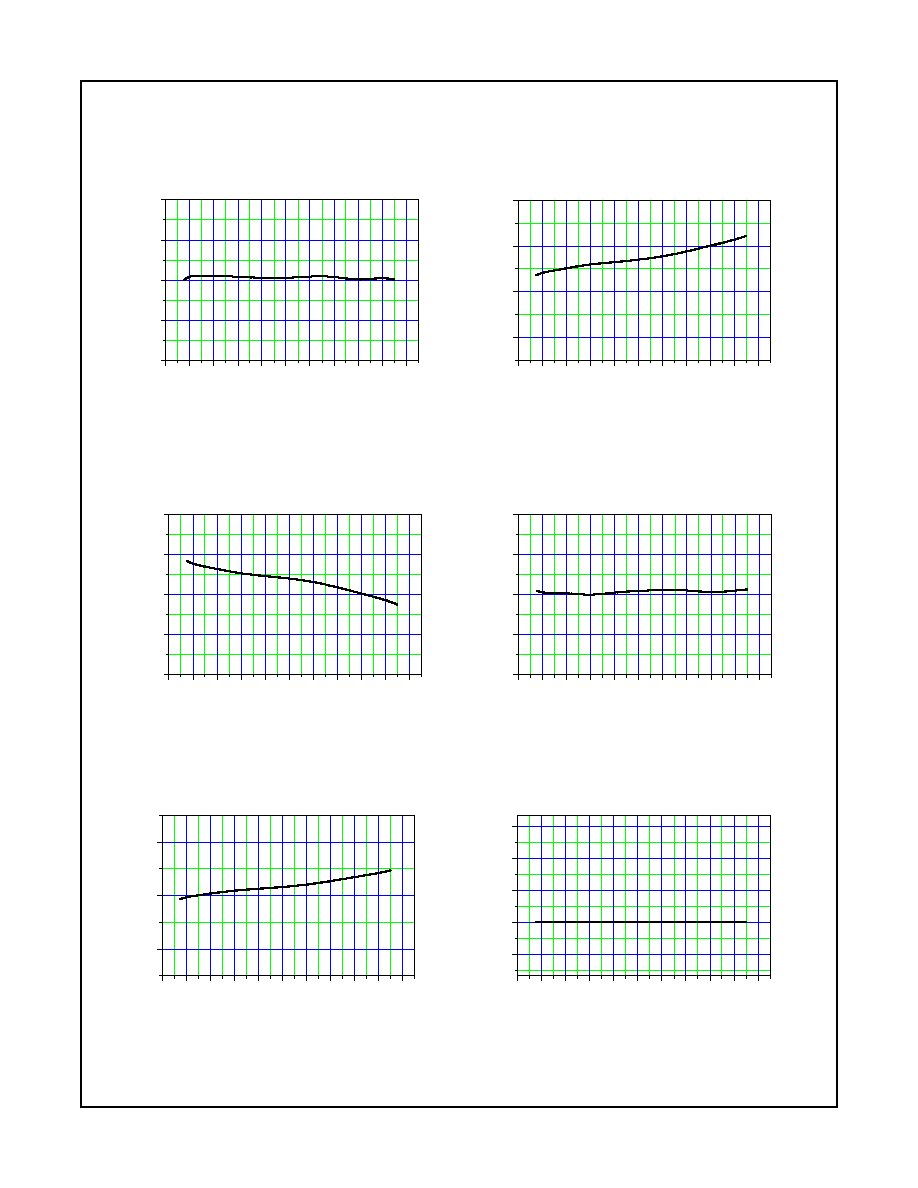
Typical Characteristics
Figure 4. Start Threshold Voltage vs. Temp.
Figure 5. Stop Threshold Voltage vs. Temp.
Figure 6. UVLO Hysteresis vs. Temp.
Figure 7. Zener Voltage vs. Temp.
Figure 8. Start-up Supply Current vs. Temp.
Figure 9. Operating Supply Current vs. Temp.
-60 -40 -20
0
20
40
60
80 100 120 140
11.0
11.5
12.0
12.5
13.0
V
th
(
s
t
a
r
t
)
[V]
Temperature [∞C]
-60 -40 -20
0
20
40
60
80 100 120 140
7.5
8.0
8.5
9.0
9.5
V
th
(
s
to
p
)
[V
]
Temperature [∞C]
-60 -40 -20
0
20
40
60
80 100 120 140
3.00
3.25
3.50
3.75
4.00
HY
(U
V
L
O
)
[V
]
Temperature [∞C]
-60 -40 -20
0
20
40
60
80 100 120 140
21.0
21.5
22.0
22.5
23.0
V
Z
[V
]
Temperature [∞C]
-60 -40 -20
0
20
40
60
80 100 120 140
15
30
45
60
I
st
[
A]
Temperature [∞C]
-60 -40 -20
0
20
40
60
80 100 120 140
0.0
0.8
1.6
2.4
I
CC
[m
A]
Temperature [∞C]

F
AN7530 Critical Conducti
on Mode PFC Controller
© 2006 Fairchild Semiconductor Corporation
www.fairchildsemi.com
FAN7530 Rev. 1.0.0
8
Typical Characteristics
(Continued)
Figure 10. Dynamic Operating Supply Current vs.
Temp.
Figure 11. Operating Current at Disable vs. Temp.
Figure 12. V
ref1
vs. Temp.
Figure 13.
V
ref1
vs. Temp.
Figure 14. Input Bias Current vs. Temp.
Figure 15. Output Source Current vs. Temp.
-60 -40 -20
0
20
40
60
80 100 120 140
0
1
2
3
4
I
dcc
[mA]
Temperature [∞C]
-60 -40 -20
0
20
40
60
80 100 120 140
36
54
72
90
I
CC
(di
s
)
[
A]
Temperature [∞C]
-60 -40 -20
0
20
40
60
80 100 120 140
2.48
2.50
2.52
V
re
f
1
[V]
Temperature [∞C]
-60 -40 -20
0
20
40
60
80 100 120 140
0.0
2.5
5.0
7.5
10.0
V
re
f
1
[m
V]
Temperature [∞C]
-60 -40 -20
0
20
40
60
80 100 120 140
-0.50
-0.25
0.00
0.25
0.50
I
b(
e
a
)
[
A]
Temperature [∞C]
-60 -40 -20
0
20
40
60
80 100 120 140
-18
-15
-12
-9
I
s
our
c
e
[
A]
Temperature [∞C]

F
AN7530 Critical Conducti
on Mode PFC Controller
© 2006 Fairchild Semiconductor Corporation
www.fairchildsemi.com
FAN7530 Rev. 1.0.0
9
Typical Characteristics
(Continued)
Figure 16. Output Sink Current vs. Temp.
Figure 17. Output Upper Clamp Voltage vs. Temp.
Figure 18. Zero Duty Cycle Output Voltage vs. Temp.
Figure 19. Maximum On-Time Voltage vs. Temp.
Figure 20. Maximum On-Time vs. Temp.
Figure 21. Current Sense Input Threshold Voltage vs.
Temp.
-60 -40 -20
0
20
40
60
80 100 120 140
6
9
12
15
18
I
si
n
k
[
A]
Temperature [∞C]
-60 -40 -20
0
20
40
60
80 100 120 140
5.4
5.7
6.0
6.3
6.6
V
eao
(H
) [
V
]
Temperature [∞C]
-60 -40 -20
0
20
40
60
80 100 120 140
0.90
0.95
1.00
1.05
1.10
V
e
ao(
Z
)
[V
]
Temperature [∞C]
-60 -40 -20
0
20
40
60
80 100 120 140
2.80
2.85
2.90
2.95
3.00
V
mo
t
[V
]
Temperature [∞C]
-60 -40 -20
0
20
40
60
80 100 120 140
21
24
27
T
on(
m
a
x
)
[
s]
Temperature [∞C]
-60 -40 -20
0
20
40
60
80 100 120 140
0.70
0.75
0.80
0.85
0.90
V
cs(
lim
it
)
[V
]
Temperature [∞C]
F
AN7530 Critical Conducti
on Mode PFC Controller
© 2006 Fairchild Semiconductor Corporation
www.fairchildsemi.com
FAN7530 Rev. 1.0.0
10
Typical Characteristics
(Continued)
Figure 22. Input Bias Current vs. Temp.
Figure 23. Input High Clamp Voltage vs. Temp.
Figure 24. Input Low Clamp Voltage vs. Temp.
Figure 25. Input Bias Current vs. Temp.
Figure 26. Maximum Output Voltage vs. Temp.
Figure 27. Output Voltage with UVLO Activated vs.
Temp.
-60 -40 -20
0
20
40
60
80 100 120 140
-1.0
-0.5
0.0
0.5
1.0
I
b
(
cs)
[
A]
Temperature [∞C]
-60 -40 -20
0
20
40
60
80 100 120 140
6.0
6.4
6.8
7.2
V
c
l
am
p(
H
)
[V
]
Temperature [∞C]
-60 -40 -20
0
20
40
60
80 100 120 140
0.00
0.25
0.50
0.75
1.00
V
c
l
am
p(
L)
[V
]
Temperature [∞C]
-60 -40 -20
0
20
40
60
80 100 120 140
-1.0
-0.5
0.0
0.5
1.0
I
b
(
zcd
)
[
A]
Temperature [∞C]
-60 -40 -20
0
20
40
60
80 100 120 140
12
13
14
V
O(m
a
x)
[V
]
Temperature [∞C]
-60 -40 -20
0
20
40
60
80 100 120 140
-0.3
0.0
0.3
0.6
0.9
V
O(
u
v
l
o
)
[V
]
Temperature [∞C]

F
AN7530 Critical Conducti
on Mode PFC Controller
© 2006 Fairchild Semiconductor Corporation
www.fairchildsemi.com
FAN7530 Rev. 1.0.0
11
Typical Characteristics
(Continued)
Figure 28. Restart Delay Time vs. Temp.
Figure 29. OVP Threshold Voltage vs. Temp.
Figure 30. OVP Hysteresis vs. Temp.
Figure 31. Enable Threshold Voltage vs. Temp.
Figure 32. Enable Hysteresis vs. Temp.
-60 -40 -20
0
20
40
60
80 100 120 140
50
100
150
200
250
300
t
d(
rs
t)
[
s]
Temperature [∞C]
-60 -40 -20
0
20
40
60
80 100 120 140
2.64
2.67
2.70
2.73
V
ov
p
[V
]
Temperature [∞C]
-60 -40 -20
0
20
40
60
80 100 120 140
0.12
0.15
0.18
0.21
HY
(OVP
)
[V]
Temperature [∞C]
-60 -40 -20
0
20
40
60
80 100 120 140
0.400
0.425
0.450
0.475
0.500
V
th(
e
n)
[V
]
Temperature [∞C]
-60 -40 -20
0
20
40
60
80 100 120 140
0.050
0.075
0.100
0.125
0.150
HY
(
en)
[V
]
Temperature [∞C]
F
AN7530 Critical Conducti
on Mode PFC Controller
© 2006 Fairchild Semiconductor Corporation
www.fairchildsemi.com
FAN7530 Rev. 1.0.0
12
Applications Information
1. Error Amplifier Block
The error amplifier block consists of a transconductance
amplifier, output OVP comparator, and disable compara-
tor. For the output voltage control, a transconductance
amplifier is used instead of the conventional voltage
amplifier. The transconductance amplifier (voltage con-
trolled current source) aids the implementation of OVP
and disable function. The output current of the amplifier
changes according to the voltage difference of the invert-
ing and non-inverting input of the amplifier. The output
voltage of the amplifier is compared with the internal
ramp signal to generate the switch turn-off signal. The
OVP comparator shuts down the output drive block when
the voltage of the INV pin is higher than 2.675V and
there is 0.175V hysteresis. The disable comparator dis-
ables the operation of the FAN7530 when the voltage of
the inverting input is lower than 0.45V and there is
100mV hysteresis. An external small signal MOSFET
can be used to disable the IC, as shown in Figure 33.
The IC operating current decreases below 65µA to
reduce power consumption if the IC is disabled.
Figure 33. Error Amplifier Block
2. Zero Current Detection Block
The zero current detector (ZCD) generates the turn-on
signal of the MOSFET when the boost inductor current
reaches zero using an auxiliary winding coupled with the
inductor. If the voltage of the ZCD pin goes higher than
1.5V, the ZCD comparator waits until the voltage goes
below 1.4V. If the voltage goes below 1.4V, the zero cur-
rent detector turns on the MOSFET. The ZCD pin is pro-
tected internally by two clamps, 6.7V-high clamp and
0.65V-low clamp. The 150µs timer generates a MOSFET
turn-on signal if the drive output has been low for more
than 150µs from the falling edge of the drive output.
Figure 34. Zero Current Detector Block
3. Sawtooth Generator Block
The output of the error amplifier and the output of the
sawtooth generator are compared to determine the
MOSFET turn-off instance. The slope of the sawtooth is
determined by an external resistor connected to the
MOT pin. The voltage of the MOT pin is 2.9V and the
slope is proportional to the current flowing out of the
MOT pin. The internal ramp signal has a 1V offset; there-
fore, the drive output is shut down if the voltage of the
COMP pin is lower than 1V. The MOSFET on-time is
maximum when the COMP pin voltage is 5V. According
to the slope of the internal ramp, the maximum on-time
can be programmed. The necessary maximum on-time
depends on the boost inductor, lowest AC line voltage,
and maximum output power. The resistor value should
be designed properly.
Figure 35. Sawtooth Generator Block
INV
Error Amp
OVP
COMP
2.675V
2.5V
3
1
Gm
0.45V
0.35V
Disable
V
out
V
ref1
(2.5V)
Disable
Signal
FAN7530 Rev. 00
Timer
ZCD
6.7V
Zero Current
Detector
R
S
Q
5
1.5V
1.4V
V
in
R
ZCD
150
s
Turn-on
Signal
FAN7530 Rev. 00
1V Offset
MOT
3
Error Amp
Output
Off Signal
2.9V
Sawtooth
Generator
FAN7530 Rev. 00
F
AN7530 Critical Conducti
on Mode PFC Controller
© 2006 Fairchild Semiconductor Corporation
www.fairchildsemi.com
FAN7530 Rev. 1.0.0
13
4. Over-Current Protection Block
The MOSFET current is sensed using an external sens-
ing resistor for the over-current protection. If the CS pin
voltage is higher than 0.8V, the over-current protection
comparator generates a protection signal. An internal RC
filter is included to filter switching noise.
Figure 36. Over-Current Protection Block
5. Switch Drive Block
The FAN7530 contains a single totem-pole output stage
designed for direct drive of the power MOSFET. The
drive output is capable of up to +500/-800mA peak cur-
rent with a typical rise and fall time of 50ns with 1nF load.
The output voltage is clamped to 13V to protect the
MOSFET gate if the V
CC
voltage is higher than 13V.
6. Under-Voltage Lockout Block
If the V
CC
voltage reaches 12V, the IC's internal blocks
are enabled and start operation. If the V
CC
voltage drops
below 8.5V, most of the internal blocks are disabled to
reduce the operating current. V
CC
voltage should be
higher than 8.5V under normal conditions.
8pF
40k
CS
Over-Current Protection
Comparator
4
0.8V
OCP
Signal
FAN7530 Rev. 00

F
AN7530 Critical Conducti
on Mode PFC Controller
© 2006 Fairchild Semiconductor Corporation
www.fairchildsemi.com
FAN7530 Rev. 1.0.0
14
Typical Application Circuit
Features
High efficiency (>90% at 85V
AC
input)
Low total harmonic distortion (THD) (<10% at 265V
AC
input, 25W load)
Key Design Notes
R1, R2, R5, C11 should be optimized for best THD characteristic.
1. Schematic
Figure 37. Schematic
Application
Output Power
Input Voltage
Output Voltage
Ballast
100W
Universal input
(85~265V
AC
)
400V
F1
AC INPUT
5
6
7
8
OUT
V
CC
GND
ZCD
INV
COMP
MOT
CS
FAN7530
1
2
3
4
V1
C1
C3
C4
LF1
C2
NTC
BD
C5
C6
R3
R4
R5
T1
D1
R7
R10
R6
D2
R9
Q1
V
AUX
R2
R11
C9
ZD1
C10
PFC OUTPUT
D3
R1
C7
R8
C8
C11
FAN7530 Rev. 00

F
AN7530 Critical Conducti
on Mode PFC Controller
© 2006 Fairchild Semiconductor Corporation
www.fairchildsemi.com
FAN7530 Rev. 1.0.0
15
2. Inductor Schematic Diagram
Figure 38. Inductor Schematic Diagram
3. Winding Specification
4. Electrical Characteristics
5. Core & Bobbin
Core: EI 3026
Bobbin: EI3026
Ae(mm
2
): 111
No
Pin (s
f)
Wire
Turns
Winding Method
N
Vcc
2
1
0.2
◊ 1
8
Solenoid Winding
Insulation: Polyester Tape t = 0.050mm, 4 Layers
Np
5
3
0.2
◊ 10
58
Solenoid Winding
Outer Insulation: Polyester Tape t = 0.050mm, 4 Layers
Air Gap: 0.6mm for each leg
Pin
Specification
Remarks
Inductance
3 - 5
600µH ± 10%
100kHz, 1V
Np
1
2
N
Vcc
5
3
FAN7530 Rev. 00

F
AN7530 Critical Conducti
on Mode PFC Controller
© 2006 Fairchild Semiconductor Corporation
www.fairchildsemi.com
FAN7530 Rev. 1.0.0
16
6. Demo Circuit Part List
Part
Value
Note
Part
Value
Note
Fuse
Inductor
F1
3A/250V
T1
600µH
EI3026
NTC
NTC
10D-9
MOSFET
Resistor
Q1
FQPF13N50C
Fairchild
R1
56k
1/4W
R2
820k
1/4W
Diode
R3
330k
1/2W
D1
1N4148
Fairchild
R4
150
1/2W
D2
BYV26C
600V, 1A
R5
20k
1/4W
D3
SB140
Fairchild
R6
10
1/4W
ZD1
1N4746
18V
R7
0.2
1/2W
R8
10k
1/4W
R9
10k
1/4W
Bridge Diode
R10
2M
1/4W
BD
KBL06
600V/4A
R11
12.9k
1/4W
Line Filter
Capacitor
LF1
40mH
Wire 0.4mm
C1
150nF/275VAC
Box Capacitor
C2
470nF/275VAC
Box Capacitor
IC
C3
2.2nF/3kV
Ceramic Capacitor
IC1
FAN7530
Fairchild
C4
2.2nF/3kV Ceramic
Capacitor
C5
TNR
C6
47µF/25V
Electrolytic Capacitor
V1
471
470V
C7
47nF/50V
Ceramic Capacitor
C8
220nF/50V
Multilayer Ceramic
Capacitor
C9
100µF/450V
Electrolytic Capacitor
C10
12nF/100V
Film Capacitor
C11
56pF/50V
Ceramic Capacitor

F
AN7530 Critical Conducti
on Mode PFC Controller
© 2006 Fairchild Semiconductor Corporation
www.fairchildsemi.com
FAN7530 Rev. 1.0.0
17
7. Layout
Figure 39. PCB Layout Considerations for FAN7530
8. Performance Data
P
OUT
85V
AC
115V
AC
230V
AC
265V
AC
100W
PF
0.998
0.998
0.991
0.984
THD
5.1%
3.6%
5.2%
6.2%
Efficiency
90.9%
93.7%
95.6%
96%
75W
PF
0.999
0.998
0.986
0.975
THD
4.1%
3.6%
5.0%
5.7%
Efficiency
91.6%
93.3%
94.6%
95.3%
50W
PF
0.998
0.997
0.974
0.956
THD
4.4%
5.0%
5.7%
6.2%
Efficiency
91.3%
91.9%
92.7%
93.4%
25W
PF
0.995
0.991
0.923
0.876
THD
7.9%
8.6%
8.3%
8.7%
Efficiency
86.4%
87.1%
87.3%
88.1%
Power Ground
Signal Ground
Separate the power ground
and the signal ground
Place the output voltage
sensing resistors close to IC
F
AN7530 Critical Conducti
on Mode PFC Controller
© 2006 Fairchild Semiconductor Corporation
www.fairchildsemi.com
FAN7530 Rev. 1.0.0
18
Mechanical Dimensions
8-DIP
Dimensions are in millimeters (inches) unless otherwise noted..
September 1999, Rev B
6.40
±
0.20
3.30
±
0.30
0.130
±
0.012
3.40
±
0.20
0.134
±
0.008
#1
#4
#5
#8
0.252
±
0.008
9.20
±
0.20
0.79
2.54
0.100
0.031
()
0.46
±
0.10
0.018
±
0.004
0.060
±
0.004
1.524
±
0.10
0.362
±
0.008
9.60
0.378
MAX
5.08
0.200
0.33
0.013
7.62
0~15
∞
0.300
MAX
MIN
0.25
+0.10
≠0.05
0.010
+0.004
≠0.002
8dip_dim.pdf

F
AN7530 Critical Conducti
on Mode PFC Controller
© 2006 Fairchild Semiconductor Corporation
www.fairchildsemi.com
FAN7530 Rev. 1.0.0
19
Mechanical Dimensions
(Continued)
8-SOP
Dimensions are in millimeters (inches) unless otherwise noted.
September 2001, Rev B1
sop8_dim.pdf
4.92
±
0.20
0.194
±
0.008
0.41
±
0.10
0.016
±
0.004
1.27
0.050
5.72
0.225
1.55
±
0.20
0.061
±
0.008
0.1~0.25
0.004~0.001
6.00
±
0.30
0.236
±
0.012
3.95
±
0.20
0.156
±
0.008
0.50
±
0.20
0.020
±
0.008
5.13
0.202
MAX
#1
#4
#5
0~8
∞
#8
0.56
0.022
()
1.80
0.071
MAX0.10
MAX0.004
MAX
MIN
+
0.10
-0.05
0.15
+
0.004
-0.002
0.006
TRADEMARKS
The following are registered and unregistered trademarks Fairchild Semiconductor owns or is authorized to use and is not intended to be an
exhaustive list of all such trademarks.
ACEx GlobalOptoisolator
OCXPro
SerDes
TinyBuck
ActiveArray
GTO
OPTOLOGIC
Æ
SILENT
SWITCHER
Æ
TinyLogic
Æ
Bottomless
HiSeC
OPTOPLANAR SMART
START TINYOPTO
Build it Now
I
2
C
PACMAN SPM TinyPower
CoolFET
i-Lo
POP Stealth TinyPWM
CROSSVOLT
ImpliedDisconnect
Power247 SuperFET TruTranslation
DOME
IntelliMAX
PowerEdge SuperSOT -3 UHC
EcoSPARK
ISOPLANAR
PowerSaver
SuperSOT -6
UltraFET
Æ
E
2
CMOS
LittleFET
PowerTrench
Æ
SuperSOT -8 UniFET
EnSigna
MICROCOUPLER
QFET
Æ
SyncFET VCX
FACT
MicroFET QS TCM Wire
FACT Quiet Series
MicroPak QT
Optoelectronics TinyBoost
FAST
Æ
MICROWIRE Quiet
Series
FASTr
MSX RapidConfigure
Across the board. Around the world.
FPS
MSXPro RapidConnect
Programmable Active Droop
FRFET
OCX ScalarPump
The Power Franchise
Æ
DISCLAIMER
FAIRCHILD SEMICONDUCTOR RESERVES THE RIGHT TO MAKE CHANGES WITHOUT FURTHER NOTICE TO ANY PRODUCTS
HEREIN TO IMPROVE RELIABILITY, FUNCTION OR DESIGN. FAIRCHILD DOES NOT ASSUME ANY LIABILITY ARISING OUT OF THE
APPLICATION OR USE OF ANY PRODUCT OR CIRCUIT DESCRIBED HEREIN; NEITHER DOES IT CONVEY ANY LICENSE UNDER
ITS PATENT RIGHTS, NOR THE RIGHTS OF OTHERS. THESE SPECIFICATIONS DO NOT EXPAND THE TERMS OF FAIRCHILD'S
WORLDWIDE TERMS AND CONDITIONS, SPECIFICALLY THE WARRANTY THEREIN, WHICH COVERS THESE PRODUCTS.
LIFE SUPPORT POLICY
FAIRCHILD'S PRODUCTS ARE NOT AUTHORIZED FOR USE AS CRITICAL COMPONENTS IN LIFE SUPPORT DEVICES OR
SYSTEMS WITHOUT THE EXPRESS WRITTEN APPROVAL OF FAIRCHILD SEMICONDUCTOR CORPORATION.
As used herein:
1.
Life support devices or systems are devices or systems
which, (a) are intended for surgical implant into the body or
(b) support or sustain life, and (c) whose failure to perform
when properly used in accordance with instructions for use
provided in the labeling, can be reasonably expected to
result in a significant injury of the user.
2.
A critical component in any component of a life support,
device, or system whose failure to perform can be
reasonably expected to cause the failure of the life
support device or system, or to affect its safety or
effectiveness.
PRODUCT STATUS DEFINITIONS
Definition of Terms
Datasheet Identification
Product Status
Definition
Advance Information
Formative or In
Design
This datasheet contains the design specifications for product
development. Specifications may change in any manner without
notice.
Preliminary
First Production
This datasheet contains preliminary data; supplementary data will
be published at a later date. Fairchild Semiconductor reserves the
right to make changes at any time without notice to improve design.
No Identification Needed
Full Production
This datasheet contains final specifications. Fairchild
Semiconductor reserves the right to make changes at any time
without notice to improve design.
Obsolete
Not In Production
This datasheet contains specifications on a product that has been
discontinued by Fairchild Semiconductor. The datasheet is printed
for reference information only.
Rev. I20
F
AN7530 Critical Conducti
on Mode PFC Controller
© 2006 Fairchild Semiconductor Corporation
www.fairchildsemi.com
FAN7530 Rev. 1.0.0
20