 | –≠–ª–µ–∫—Ç—Ä–æ–Ω–Ω—ã–π –∫–æ–º–ø–æ–Ω–µ–Ω—Ç: FAN7548 | –°–∫–∞—á–∞—Ç—å:  PDF PDF  ZIP ZIP |

©2003 Fairchild Semiconductor Corporation
www.fairchildsemi.com
Rev. 1.0.0
Features
∑ Backlight Lamp Ballast and Soft Dimming
∑ Reduce the Number of Components
∑ Wide Range Operating Voltage 9-30V
∑ Precision Voltage Reference Trimmed to 3.4%
∑ Low Standby Current (Typ. 150uA)
∑ Soft Start Function
∑ Dual PWM Control
∑ Analog & Burst Dimming Function
∑ P-Channel MOSFET Drive
∑ Open Lamp Regulation(OLR)
∑ Open Lamp Protection(OLP)
∑ Buck+Royer Topology
∑ 20 SSOP
Description
The FAN7548 provides the necessary circuit blocks to
implement a highly efficient CCFL backlight power supply
in a small footpirnt 20 SSOP package. The device features
two control stages for operating independent resonant tanks
for multi-lamp designs.
External parts count is minimized and system cost is reduced
by integration such features as a feedback controlled PWM
driver stage, the soft start, the open lamp regulation, the open
lamp protection, the UVLO, and the self-synchronization
circuitry between the buck and Royer stages. It includes an
internal shunt regulator, allowing it to operate with input
voltage from 9 to 30V. It supports analog and burst dimming
modes of operation. It providees the open lamp regulation,
and the open lamp protection.
20-SSOP
1
FAN7548
FAN7548
FAN7548
FAN7548
Dual LCD Back Light Inverter Drive IC
Dual LCD Back Light Inverter Drive IC
Dual LCD Back Light Inverter Drive IC
Dual LCD Back Light Inverter Drive IC
FAN7548
2
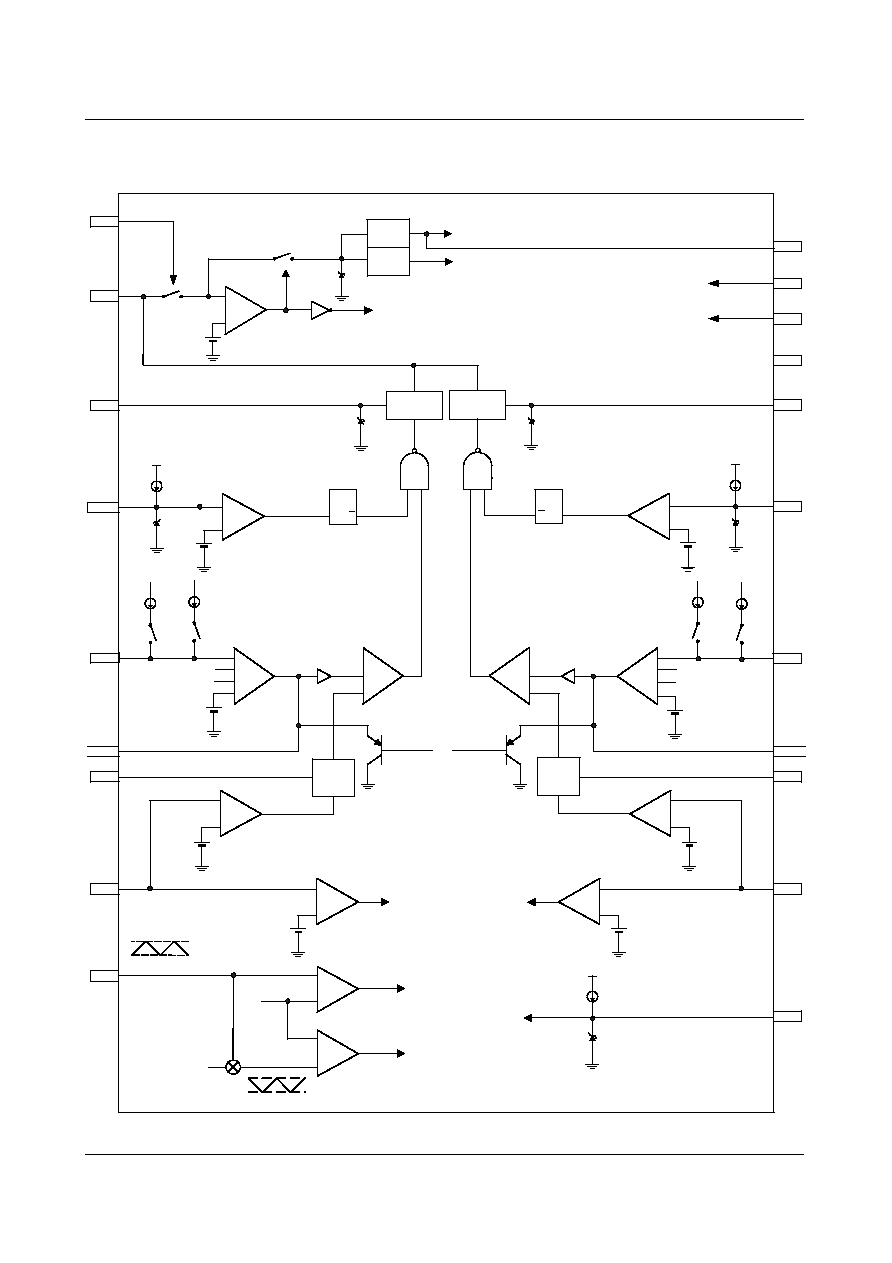
Internal Block Diagram
ADIM
-
+
OLP2
R
S
Vb
Va
COMP6
3.7V
Vz
2uA
Q
2.5V
Output
Drive2
-
-
-
-
+
+
+
+
COMP5
BCT
OUT2
Vb
-
+
OLP1
R
S
COMP1
3.7V
Vz
2uA
Buffer
Error Amp.1
Q
-
+
-
+
2.5V
6V
OLR1
VFB1
COMP1
OSC1
Output
Drive1
OUT1
COMP4
COMP3
Va
-
+
1.5V
COMP2
-
+
Vcc
3Vref
Internal
Bias
ENA
Vz
5.2V
UVLO
V3
BDIM
Min. 0.25V
Max. 1.75V
S
OLR1
S
Burst1
Buffer
Error Amp.2
-
+
-
+
OLR2
VFB2
COMP2
OSC2
COMP9
COMP8
Va
-
+
1.5V
COMP7
S
OLR2
S
Burst2
To S
OLR1
To S
Burst1
S
OLR2
Vcc
10uA
6.5V
CSS
Css
To S
Burst2
GND
13.5V
13.5V
-
+
+
-
+
+
2.5V
2.5V
-
-
-
-
+
+
+
+
COMP10
+
+
+
+
-
-
-
-
(Max.+Min.) of BCt
Sync.
Sync.
Ramp
Ramp
6V
+
Css
Css
+
Css
Min. 0.25V
Max. 1.75V
FAN7548
3
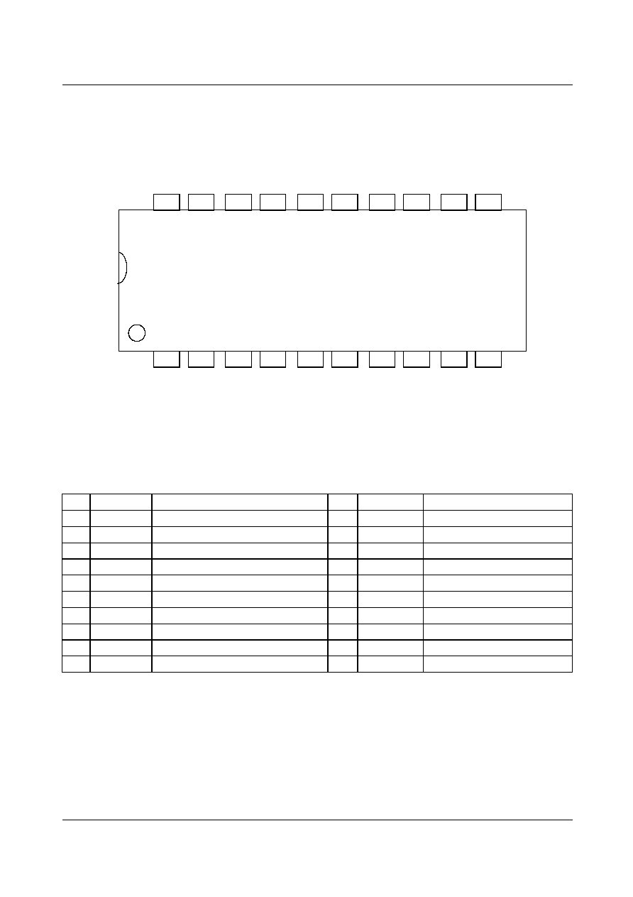
Pin Assignments
Pin Definitions
No
Name
Function Description
No
Name
Function Description
1
BDIM
Burst Dimming Input
11
OUT2
Gate Dirve Output 2
2
BCT
Timing Capacitor for Burst Dimming
12
GND
Ground
3
OLP1
Open Lamp Protection 1
13
CSS
Capacitor for Soft Start
4
VFB1
Error Amp Input 1
14
OSC2
Main Oscillator 2
5
COMP1
Error Amp Output 1
15
OLR2
Open Lamp Regulation 2
6
OLR1
Open Lamp Regulation 1
16
COMP2
Error Amp Output 2
7
OSC1
Main Oscillator 1
17
VFB2
Error Amp Input 2
8
ENA
ON/OFF Control Input
18
OLP2
Open Lamp Protection 2
9
VCC
Power Supply
19
ADIM
Analog Dimming Input
10
OUT1
Gate Drive Output 1
20
V3
3V Reference Voltage
20
10
6
5
4
3
2
1
11
12
13
14
15
16
17
18
19
9
8
7
FAN 7 5 4 8

FAN7548
4
Absolute Maximum Ratings
Vcc=12V, Ta=25
∞
C for typical values and -25
∞
C
Ta
85
∞
C and 9V
Vcc
30V for min/max values,
unless otherwise specified.
Note:
1. Thermal resistance test board
Size: 76.2mm * 114.3mm * 1.6mm(1S0P)
JEDEC standard: JESD51-3, JESD51-7
2. Assume no ambient airflow
Characteristics
Symbol
Value
Unit
Supply Voltage
V
CC
6~30
V
Operating Temperature Range
Topr
-25 ~ 85
∞
C
Storage Temperature Range
Tstg
-65 ~ 150
∞
C
Thermal Resistance Junction-Air (Note1,2)
R
JA
112
∞
C/W
Power Dissipation
Pd
1.1
W

FAN7548
5
Electrical Characteristics
Vcc=12V, Ta=25
∞
C for typical values and -25
∞
C
Ta
85
∞
C and 9V
Vcc
30V for min/max values,
unless otherwise specified.
Characteristics
Symbol
Test Condition
Min.
Typ.
Max.
Unit
ON/OFF SECTION
On Stage Input Voltage
Von
-
0.7
-
1.7
V
SOFT START SECTION
Soft Start Charging Current
I
ss
Css=4V
8.5
10
11.5
uA
Soft Start Clamping High Voltage
Vssh
-
5.5
6.5
7.5
V
UVLO SECTION
Start Up Current
Ist
Vcc=4.5V
-
100
300
uA
Start Threshold Voltage
Vst
-
4.7
5.2
5.7
V
Operating Supply Current
Iop
Vcc=12V
7
10
13
mA
REFERENCE SECTION
3V Reference Voltage
V3
-
2.88
2.98
3.08
V
Refrence Voltage
Vref
-
2.425
2.5
2.575
V
ERROR AMP SECTION
Output Sink Current
lsin
COMP=3V
-
-
-2
mA
Output Source Current
lsur
COMP=3V
2
-
-
mA
BURST OSCILLATOR SECTION
Operating Frequency
Fbosc
Ct=150n
93
110
127
Hz
Osc High Voltage
Vbh
-
-
1.75
-
V
Osc Low Voltage
Vbl
-
-
0.25
-
V
PROTECTION SECTION
Open Lamp Regulation Voltage
Vor
-
5.5
6
6.5
V
Open Lamp Protection Voltage
Vpr
-
2
2.5
3
V
Open Lamp Protection Current
Ipr
-
-
2.5
-
uA
OUTPUT SECTION
Output High Voltage
Voh
Vcc=12V
10
-
-
V
Output Low Voltage
Vol
Vcc=12V
-
-
0.2
V
Output Clamping High Voltage
Voch
V
CC
= 15V
11.5
13.5
15.5
V
Output Voltage with UVLO Activated
Vuv
V
CC
= 4V
2
-
4
V
Rising Time
Tr
V
CC
= 12V
-
150
200
ns
Falling Time
Tf
V
CC
= 12V
-
100
150
ns