 | ÐлекÑÑоннÑй компоненÑ: FAN7602 | СкаÑаÑÑ:  PDF PDF  ZIP ZIP |
Äîêóìåíòàöèÿ è îïèñàíèÿ www.docs.chipfind.ru
©2006 Fairchild Semiconductor Corporation
1
www.fairchildsemi.com
April 2006
FAN7602 Rev. 1.0.1
F
AN76
02 Green Current
Mode PWM Controller
FAN7602
Green Current Mode PWM Controller
Features
Green Current Mode PWM Control
Fixed 65kHz Operation with Frequency Modulation
Internal High-Voltage Start-up Switch
Burst Mode Operation
Line Voltage Feed Forward to Limit Maximum Power
Line Under-Voltage Protection
Latch Protection & Internal Soft-Start (10ms) Function
Overload Protection
Over Voltage Protection
Low Operation Current: Typ. 1mA
8-pin DIP
Applications
Adapter
LCD Monitor Power
Auxiliary Power Supply
Related Application Notes
AN6014 - Green Current Mode PWM Controller
FAN7602
Description
The FAN7602 is a green current mode PWM controller.
It is specially designed for off-line adapter application,
DVDP, VCR, LCD monitor application, and auxiliary
power supplies.
The internal high-voltage start-up switch and the burst
mode operation reduce the power loss in standby mode.
Because of the internal start-up switch and the burst
mode, it is possible to supply 0.5W load limiting the input
power under 1W when the input line voltage is 265Vac.
On no-load condition, the input power is under 0.3W.
The maximum power can be limited constantly, regard-
less of the line voltage change using the power limit
function.
The switching frequency is internally fixed to be 65kHz
and the frequency modulation technique reduces EMI.
The FAN7602 includes various protections for the sys-
tem reliability and the internal soft start prevents the out-
put voltage over-shoot at start-up.
Ordering Information
Part Number
Operating Temp.
Range
Pb-Free
Package Packing
Method
Marking
Code
FAN7602N
-25
°C to +125°C
Yes
8-DIP
Rail
FAN7602
2
www.fairchildsemi.com
FAN7602 Rev. 1.0.1
F
AN7602 Green Curren
t Mode PWM Controller
Typical Application Diagram
Figure 1. Typical Flyback Application
FAN7602
Internal Block Diagram
Figure 2. Functional Block Diagram of FAN7602
Soft
Start
Delay
Circuit
GND
Plimit
Offset
5V Ref
Vcc
LUVP
OUT
CS/FB
UVLO
LUVP
6
19V
OVP
12V/8V
5
3
0.95V/0.88V
8
1
Reset
Circuit
4
Vstr
2V/1.5V
4V
Latch/
Plimit
2
Plimit
Offset
Generator
Driver
Circuit
Latch
OLP
OLP
10ms
Soft Start
SS End
65kHz Clock
with
Frequency
Modulation
Auto Restart
Protection
Latch
Protection
Latch
OVP
OLP
PWM
Block
Power Limit
Soft
Start
PWM+
Plimit
Offset
Plimit
Offset
Vcc
SS End
3
www.fairchildsemi.com
FAN7602 Rev. 1.0.1
F
AN7602 Green Curren
t Mode PWM Controller
Pin Assignments
Figure 3. Pin Configuration (Top View)
Pin Definitions
Pin Number Pin Name
Pin Function Description
1
LUVP
Line Under Voltage Protection Pin. This pin is used to protect the set when the
input voltage is lower than the rated input voltage range.
2
Latch/Plimit
Latch Protection and Power Limit Pin. When the pin voltage exceeds 4V, the latch
protection works and the latch protection is reset when the Vcc voltage is lower than
5V. For the power limit function, the OCP level decreases as the pin voltage
increases.
3
CS/FB
Current Sense and Feedback Pin. This pin is used to sense the MOSFET current
for the current mode PWM and OCP. The output voltage feedback information and
the current sense information are added using external RC filter.
4
GND
Ground Pin. This pin is used for the ground potential of all the pins. For proper oper-
ation, the signal ground and the power ground should be separated.
5
OUT
Gate Drive Output Pin. This pin is an output pin to drive an external MOSFET. The
peak sourcing current is 450mA and the peak sinking current is 600mA. For proper
operation, the stray inductance in the gate driving path must be minimized.
6
Vcc
Supply Voltage Pin. IC operating current and MOSFET driving current are supplied
using this pin.
7
NC
No Connection.
8
Vstr
Start-up Pin. This pin is used to supply IC operating current during IC start-up. After
start-up, the internal JFET is turned off to reduce power loss.
F A N 7 6 0 2
1
2
6
5
8
7
Y W W
3
4
Latch/
Plimit
GND
CS/FB
LUVP
Vstr
NC
Vcc
Out
4
www.fairchildsemi.com
FAN7602 Rev. 1.0.1
F
AN7602 Green Curren
t Mode PWM Controller
Absolute Maximum Ratings
The "Absolute Maximum Ratings" are those values beyond which the safety of the device cannot be guaranteed. The
device should not be operated at these limits. The parametric values defined in the Electrical Characteristics tables
are not guaranteed at the absolute maximum ratings. The "Recommended Operating Conditions" table defines the
conditions for actual device operation.
Thermal Impedance
Note:
1. Regarding the test environment and PCB type, please refer to JESD51-2 and JESD51-10.
Symbol
Parameter
Value
Unit
Vcc
Supply Voltage
20
V
I
OH
, I
OL
Peak Drive Output Current
+450/-600
mA
V
CS/FB
CS/FB Input Voltage
-0.3 to 20
V
V
LUVP
LUVP Input Voltage
-0.3 to 10
V
V
Latch
Latch/Plimit Input Voltage
-0.3 to 10
V
Vstr
Vstr Input Voltage
600
V
Tj
Operating Junction Temperature
150
°C
Topr
Operating Temperature Range
-25 to 125
°C
Tstg
Storage Temperature Range
-55 to 150
°C
P
D
Power Dissipation
1.2
W
V
ESD_HBM
ESD Capability, Human Body Model
2.0
kV
V
ESD_MM
ESD Capability, Machine Model
300
V
V
ESD_CDM
ESD Capability, Charged Device Model
500
V
Symbol
Parameter
Value
Unit
R
ja
Thermal Resistance, Junction to Ambient
8-DIP
100
°C/W
5
www.fairchildsemi.com
FAN7602 Rev. 1.0.1
F
AN7602 Green Curren
t Mode PWM Controller
Electrical Characteristics
(Vcc = 14V, T
A
= -25
°C~125°C, unless otherwise specified)
Note:
1. These parameters, although guaranteed by design, are not tested in mass production.
Symbol
Parameter Condition
Min.
Typ.
Max.
Unit
START UP SECTION
I
str
Vstr Start-up Current
V
str
= 30V,
T
A
= 25
°C
0.7
1
1.4
mA
UNDER VOLTAGE LOCK OUT SECTION
Vth(start)
Start Threshold Voltage
Vcc increasing
11
12
13
V
Vth(stop)
Stop Threshold Voltage
Vcc decreasing
7
8
9
V
HY(uvlo)
UVLO Hysteresis
3.6
4
4.4
V
SUPPLY CURRENT SECTION
Ist
Start-up Supply Current
T
A
= 25
°C
-
250
320
A
Icc
Operating Supply Current
Output no switching
-
1
1.5
mA
SOFT START SECTION
Tss
Soft Start Time
(1)
5
10
15
ms
PWM SECTION
F
OSC
Operating Frequency
V
CS/FB
= 0.2V,
T
A
= 25
°C
59
65
73
kHz
F
Frequency Modulation
-
±2
-
kHz
V
CS/FB1
CS/FB Threshold Voltage
T
A
= 25
°C
0.9
1.0
1.1
V
T
D
Propagation Delay to Output
(1)
-
100
150
ns
D
MAX
Maximum Duty Cycle
70
75
80
%
D
MIN
Minimum Duty Cycle
-
-
0
%
BURST MODE SECTION
V
CS/FB2
Burst On Threshold Voltage
T
A
= 25
°C
0.84
0.95
1.06
V
V
CS/FB3
Burst Off Threshold Voltage
T
A
= 25
°C
0.77
0.88
0.99
V
POWER LIMIT SECTION
K
Plimit
Offset Gain
V
Latch/Plimit
= 2V,
T
A
= 25
°C
0.12
0.16
0.20
OUTPUT SECTION
V
OH
Output Voltage High
T
A
= 25
°C, Isource = 100mA
11.5
12
14
V
V
OL
Output Voltage Low
T
A
= 25
°C, Isink = 100mA
-
1
2.5
V
Tr
Rising Time
(1)
T
A
= 25
°C, Cl = 1nF
-
45
150
ns
Tf
Falling Time
(1)
T
A
= 25
°C, Cl = 1nF
-
35
150
ns
6
www.fairchildsemi.com
FAN7602 Rev. 1.0.1
F
AN7602 Green Curren
t Mode PWM Controller
Electrical Characteristics
(Continued)
(Vcc = 14V, T
A
= -25
°C~125°C, unless otherwise specified)
Note:
1. These parameters, although guaranteed by design, are not tested in mass production.
Symbol Parameter
Condition
Min.
Typ.
Max.
Unit
PROTECTION SECTION
V
Latch
Latch Voltage
3.6
4
4.4
V
T
OLP
Overload Protection Time
(1)
20
22
24
ms
T
OLP_ST
Overload Protection Time at Start-
up
30
37
44
ms
V
OLP
Overload Protection Level
-
0
0.1
V
V
LUVPoff
Line Under-Voltage Protection On
to Off
T
A
= 25
°C
1.9
2
2.1
V
V
LUVPon
Line Under-Voltage Protection Off
to On
T
A
= 25
°C
1.4
1.5
1.6
V
V
OVP
Over Voltage Protection
T
A
= 25
°C
18
19
20
V
7
www.fairchildsemi.com
FAN7602 Rev. 1.0.1
F
AN7602 Green Curren
t Mode PWM Controller
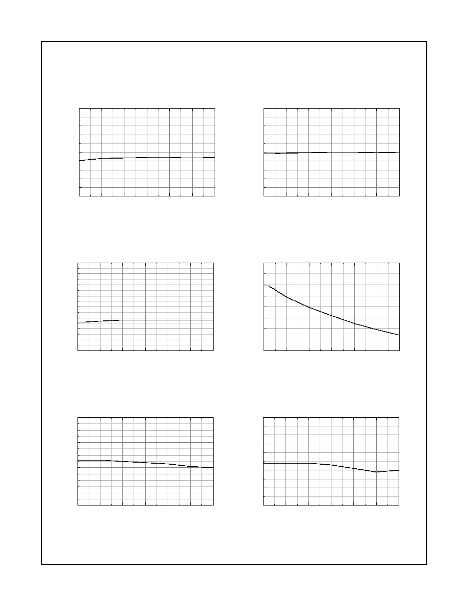
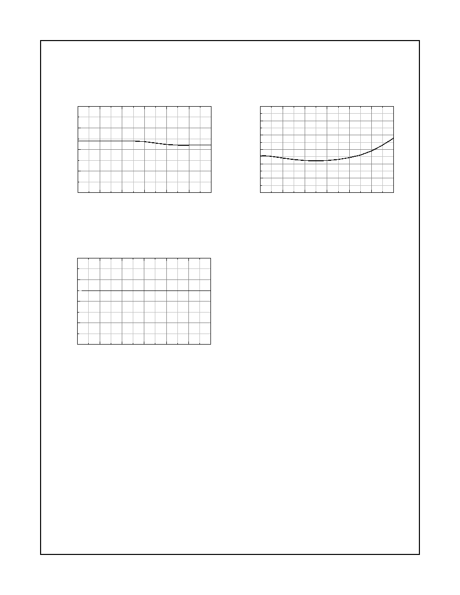
Typical Performance Characteristics
Figure 4. Start Threshold Voltage vs. Temp.
Figure 6. UVLO Hysteresis vs. Temp.
Figure 8. Operating Supply Current vs. Temp.
Figure 5. Stop Threshold Voltage vs. Temp.
Figure 7. Start-up Supply Current vs. Temp.
Figure 9. Vstr Star-up Current vs. Temp.
-25
0
25
50
75
100
125
11.2
11.6
12.0
12.4
12.8
V
TH
[V
]
Temperature
[°C]
-25
0
25
50
75
100
125
3.6
3.7
3.8
3.9
4.0
4.1
4.2
4.3
4.4
UV
LO Hy
steresi
s
[
V
]
Temperature
[°C]
-25
0
25
50
75
100
125
0.8
0.9
1.0
1.1
1.2
1.3
1.4
1.5
Io
p
[m
A]
Temperature
[°C]
-25
0
25
50
75
100
125
7.2
7.6
8.0
8.4
8.8
V
TL
[V
]
Temperature
[°C]
-25
0
25
50
75
100
125
150
200
250
300
350
Is
t [u
A
]
Temperature
[°C]
-25
0
25
50
75
100
125
0.8
0.9
1.0
1.1
1.2
1.3
Is
t
r
[m
A]
Temperature
[°C]
8
www.fairchildsemi.com
FAN7602 Rev. 1.0.1
F
AN7602 Green Curren
t Mode PWM Controller
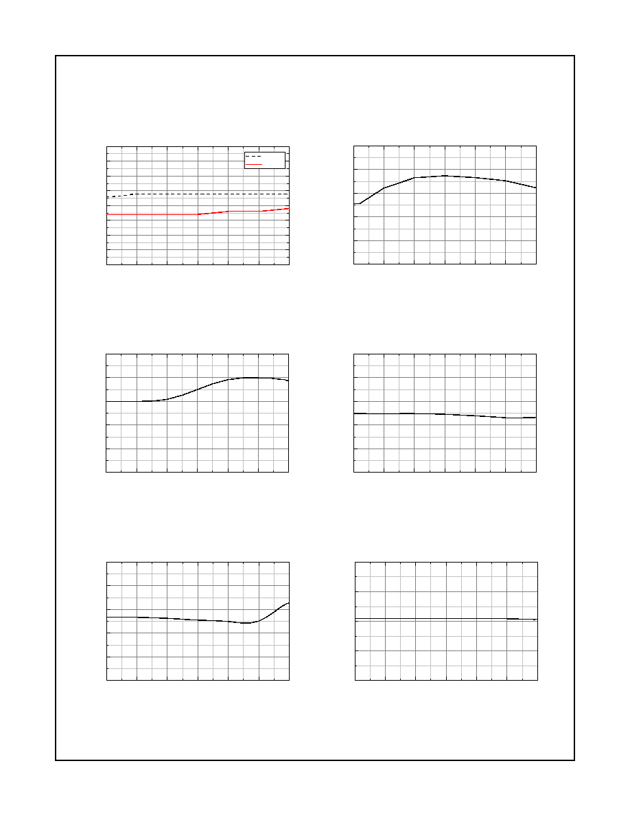
Typical Performance Characteristics
(Continued)
Figure 10. Burst On/Off Voltage vs. Temp.
Figure 12. Offset Gain vs. Temp.
Figure 14. OVP Voltage vs. Temp.
Figure 11. Operating Frequency vs. Temp.
Figure 13. Maximum Duty Cycle vs. Temp.
Figure 15. Latch Voltage vs. Temp.
-25
0
25
50
75
100
125
0.70
0.75
0.80
0.85
0.90
0.95
1.00
1.05
1.10
C
S
/
F
B T
h
r
e
shold
[
V
]
Temperature
[°C]
CSFB2
CSFB3
-25
0
25
50
75
100
125
0.10
0.12
0.14
0.16
0.18
0.20
Kp
l
i
m
i
t
Temperature
[°C]
-25
0
25
50
75
100
125
18.0
18.4
18.8
19.2
19.6
20.0
V
OVP
[
V
]
Temperature
[°C]
-25
0
25
50
75
100
125
60
62
64
66
68
70
Fos
c
[
k
H
z
]
Temperature
[°C]
-25
0
25
50
75
100
125
70
72
74
76
78
80
Dm
a
x
[%
]
Temperature
[°C]
-25
0
25
50
75
100
125
3.6
3.8
4.0
4.2
4.4
V
LATC
H
[
V
]
Temperature
[°C]
9
www.fairchildsemi.com
FAN7602 Rev. 1.0.1
F
AN7602 Green Curren
t Mode PWM Controller
Typical Performance Characteristics
(Continued)
Figure 16. LUVP On to Off Voltage vs. Temp.
Figure 18. CS/FB Threshold Voltage vs. Temp.
Figure 17. LUVP Off to On Voltage vs. Temp.
-25
0
25
50
75
100
125
1.90
1.95
2.00
2.05
2.10
V
LU
VPoff
[
V
]
Temperature
[°C]
-25
0
25
50
75
100
125
0.92
0.96
1.00
1.04
1.08
CS
FB
1
Thresh
ol
d vo
l
t
ag
e [V
]
Temperature
[°C]
-25
0
25
50
75
100
125
1.40
1.45
1.50
1.55
1.60
1.65
1.70
V
LU
VPon
[
V
]
Temperature
[°C]
10
www.fairchildsemi.com
FAN7602 Rev. 1.0.1
F
AN7602 Green Curren
t Mode PWM Controller
Applications Information
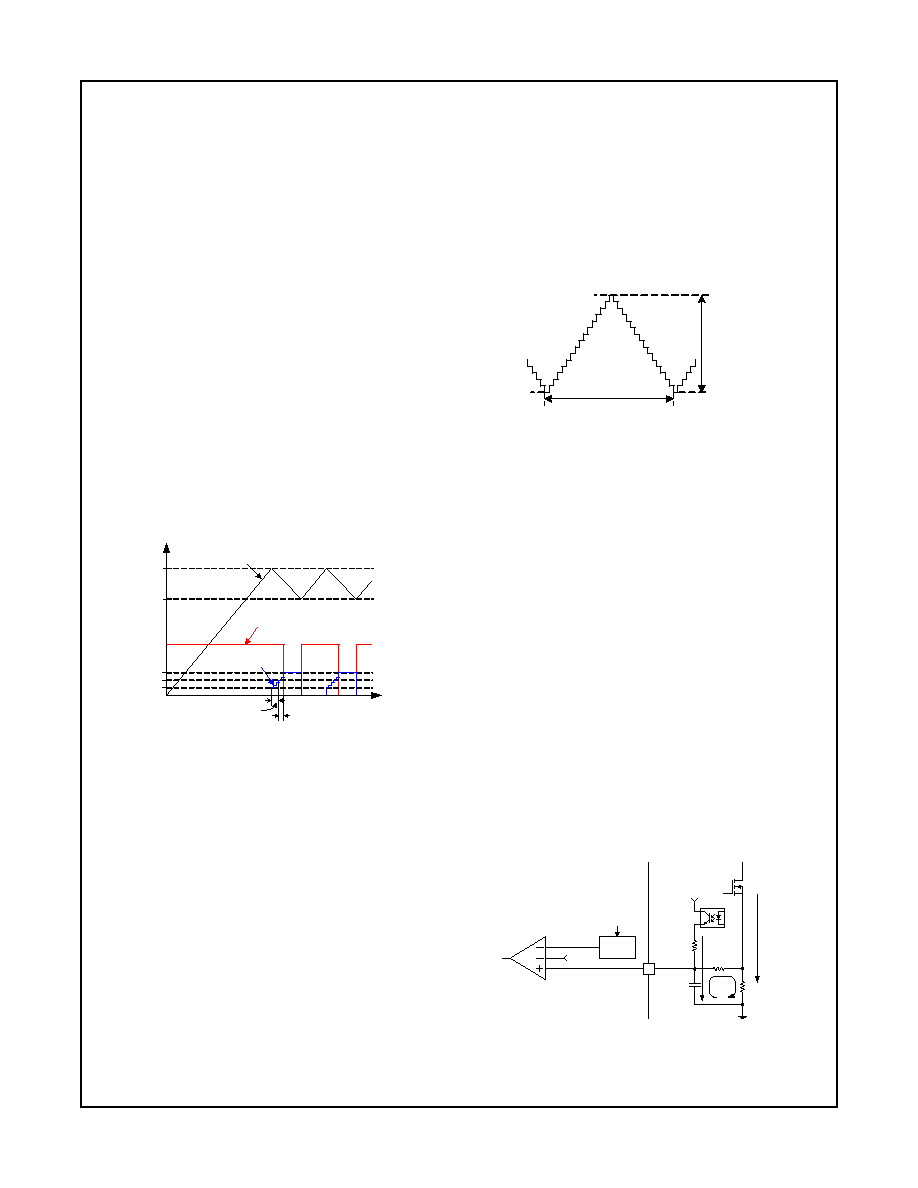
1. Start-up Circuit and Soft Start Block
The FAN7602 contains a start-up switch to reduce the
power loss of the external start-up circuit of the conven-
tional PWM converters. The internal start-up circuit
charges the Vcc capacitor with 0.9mA current source if
the AC line is connected. The start-up switch is turned off
15ms after IC starts up, as shown in Fig. 19. The soft-
start function starts when the Vcc voltage reaches the
start threshold voltage of 12V and ends when the inter-
nal soft-start voltage reaches 1V. The internal start-up
circuit starts charging the Vcc capacitor again if the Vcc
voltage is lowered to the minimum operating voltage, 8V.
The UVLO block shuts down the output drive circuit and
some blocks to reduce the IC operating current and the
internal soft-start voltage drops to zero. If the Vcc volt-
age reaches the start threshold voltage, the IC starts
switching again and the soft start block works as well.
During the soft start, pulse-width modulated (PWM) com-
parator compares the CS/FB pin voltage with the soft
start voltage. The soft-start voltage starts from 0.5V and
the soft-start ends when it reaches 1V and the soft-start
time is 10ms. The start-up switch is turned off when the
soft start voltage reaches 1.5V.
Figure 19. Start-up Current and Vcc Voltage
2. Oscillator Block
The oscillator frequency is set internally and a frequency
modulation (FM) function reduces EMI. The average fre-
quency is 65kHz and the modulation frequency is
±2kHz.
The frequency varies from 63kHz to 67kHz with 16
steps. The frequency step is 250Hz and FM frequency is
125Hz, as shown in Fig. 20.
3. Current Sense and Feedback Block
The FAN7602 performs the current sensing for the cur-
rent mode PWM and the output voltage feedback with
only one pin, pin3. To achieve the two functions with one
pin, an internal LEB (leading edge blanking) circuit to fil-
ter the current sense noise is not included because the
external RC filter is necessary to add the output voltage
feedback information and the current sense information.
Fig. 21 shows the current sense and feedback circuits.
R
S
is the current sense resistor to sense the switch cur-
rent. The current sense information is filtered by an RC
filter composed of R
F
and C
F
. According to the output
voltage feedback information, I
FB
charges or stops
charging C
F
to adjust the offset voltage. If I
FB
is zero, C
F
is discharged through R
F
and R
S
to lower the offset volt-
age.
Figure 20. Frequency Modulation
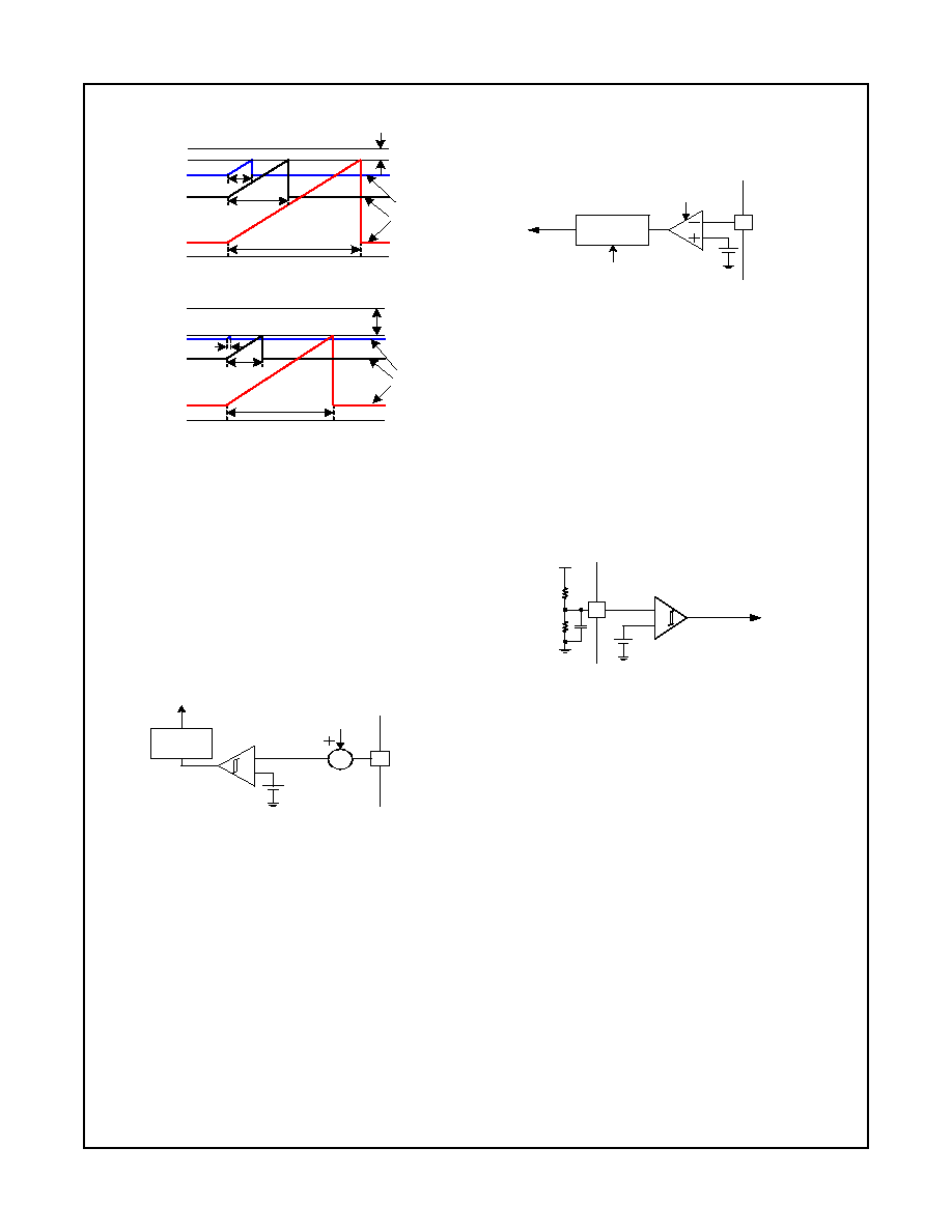
Figure 22 shows typical voltage waveforms of the CS/FB
pin. The current sense waveform is added to the offset
voltage as shown in the figure. The CS/FB pin voltage is
compared with PWM
+ that is 1V - Plimit offset as shown
in Fig. 22. If the CS/FB voltage meets PWM+, the output
drive is shut off. As shown in Fig. 22, if the feedback off-
set voltage is low, the switch on time is increased. If the
feedback offset voltage is high, then the switch on time is
decreased. In this way, the duty cycle is controlled
according to the output load condition. In general, the
maximum output power increases as the input voltage
increases because the current slope during switch on-
time increases. To limit the output power of the converter
constantly, the power limit function is included in the
FAN7602. Sensing the converter input voltage through
the Latch/Plimit pin, the Plimit offset voltage is sub-
tracted from 1V. As shown in Fig. 22, the Plimit offset
voltage is subtracted from 1V and the switch on-time
decreases as the Plimit offset voltage increases. If the
converter input voltage increases, the switch on-time
decreases, controlling the output power constant. The
offset voltage is proportional to the Latch/Plimit pin volt-
age and the gain is 0.16; if the Latch/Plimit voltage is 1V,
the offset voltage is 0.16V.
Figure 21. Current Sense and Feedback Circuits
t
Soft Start
Time (10ms)
12V
8V
Vcc
Start-up
Current
Soft Start
Voltage
1V
1.5V
0.5V
5ms
63kHz
67kHz
16 steps
1 step=250Hz
125Hz
Soft
Start
CS/FB
3
PWM
Comparator
Vcc
C
F
R
F
R
S
R
FB
I
FB
Isw
Plimit
Offset
Power
Limit
PWM+
11
www.fairchildsemi.com
FAN7602 Rev. 1.0.1
F
AN7602 Green Curren
t Mode PWM Controller
Figure 22. CS/FB Pin Voltage Waveforms
4. Burst Mode Block
The FAN7602 contains the burst mode block to reduce
the power loss at a light load and no load as the
FAN7601. A hysteresis comparator senses the offset
voltage of the Burst+ for the burst mode as shown in Fig.
23. The Burst+ is the sum of the CS/FB voltage and
Plimit offset voltage. The FAN7602 enters the burst
mode when the offset voltage of the Burst+ is higher
than 0.95V and exits the burst mode when the offset volt-
age is lower than 0.88V. The offset voltage is sensed
during the switch off time.
Figure 23. Burst Mode Block
5
. Protection Block
The FAN7602 contains several protection functions to
improve system reliability.
5.1 Overload Protection
(OLP)
The FAN7602 contains the overload protection function.
If the output load is higher than the rated output current,
the output voltage drops and the feedback error amplifier
is saturated. The offset of the CS/FB voltage represent-
ing the feedback information is almost zero. As shown in
Fig. 24, the CS/FB voltage is compared with 50mV refer-
ence when the internal clock signal is high and, if the
voltage is lower than 50mV, the OLP timer starts count-
ing. If the OLP condition persists for 22ms, the timer gen-
erates the OLP signal. And this protection is reset by the
UVLO. The OLP block is enabled after the soft start fin-
ishes.
Figure 24. Overload Protection Circuit
5.2 Line Under Voltage Protection
If the input voltage of the converter is lower than the min-
imum operating voltage, the converter input current
increases too much, causing component failure. There-
fore, if the input voltage is low, the converter should be
protected. In the FAN7602, the LUVP circuit senses the
input voltage using the LUVP pin and, if this voltage is
lower than 2V, the LUVP signal is generated. The com-
parator has 0.5V hysteresis. If the LUVP signal is gener-
ated, the output drive block is shut down, the output
voltage feedback loop is saturated, and the OLP works if
the LUVP condition persists more than 22ms.
Figure 25. Line UVP Circuit
5.3 Latch Protection
The latch protection is provided to protect the system
against abnormal conditions using the Latch/Plimit pin.
The Latch/Plimit pin can be used for the output over-
voltage protection and/or other protections. If the Latch/
Plimit pin voltage is made higher than 4V by an external
circuit, the IC is shut down. The latch protection is reset
when the Vcc voltage is lower than 5V.
5.4 Over-Voltage Protection
(OVP)
If the Vcc voltage reaches 19V, the IC shuts down and
the OVP protection is reset when the Vcc voltage is
lower than 5V.
6. Output Drive Block
The FAN7602 contains a single totem-pole output stage
to drive a power MOSFET. The drive output is capable of
up to 450mA sourcing current and 600mA sinking cur-
rent with typical rise and fall time of 45ns, 35ns respec-
tively with a 1nF load.
PWM+
CS/FB
GND
On Time
FB
Offset
1V
Power
Limit
Offset
(a) Low Power Limit Offset Case
PWM+
CS/FB
GND
On Time
FB
Offset
1V
Power
Limit
Offset
(b) High Power Limit Offset Case
C S /F B
D e la y
C ircu it
3
+
-
0 .9 5 V /0 .8 8 V
B u rst+
O ffse t
O LP
50mV
22ms
Timer
S oft S tart
C lock
C S /F B
3
2V/1.5V
1
+
-
LUVP
Vin
12
www.fairchildsemi.com
FAN7602 Rev. 1.0.1
F
AN7602 Green Curren
t Mode PWM Controller
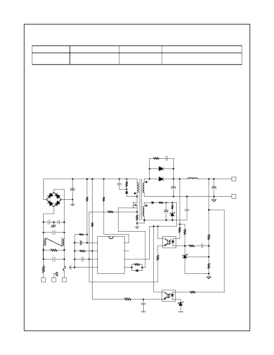
Typical application circuit
Features
Low stand-by power (<0.3W @ 265Vac)
Constant output power control
Key Design Notes
All the IC-related components should be placed close to IC, especially C107 and C110.
If R106 value is too low, there can be subharmonic oscillation.
R109 should be designed carefully to make the Vcc voltage higher than 8V when the input voltage is 265Vac at no
load.
R110 should be designed carefully to make the Vcc voltage lower than OVP level when the input voltage is 85Vac at
full load.
R103 should be designed to keep the MOSFET Vds voltage lower than maximum rating when the output is shorted.
1. Schematic
Figure 26. Schematic
Application
Output power
Input voltage
Output voltage
Adapter
48W
Universal input
(85~265Vac)
12V
FUSE
AC INPUT
C101
LF1
C102
RT
1
0
1
BD101
C105
C202
D204
L201
R204
R1
03
R101
5
6
7
8
NC
Vstr
Vcc
Out
LUVP
CS/FB
Latch/
Plimit
GND
FAN
7
602
1
2
3
4
R205
C203
R203
R202
R
201
C201
D102
IC201
OP1
R111
R104
D103
R106
Q101
T1
C1
06
D101
R105
IC101
C110
R113
C107
C204
R206
D202
C109
C103 C104
C222
1
2
3
4
C108
5
6
1
3
12
9
R207
ZD201
R108
OP2
1
2
3
4
R109
R112
R102
R107
1
2
3
R110
ZD101
R114
13
www.fairchildsemi.com
FAN7602 Rev. 1.0.1
F
AN7602 Green Curren
t Mode PWM Controller
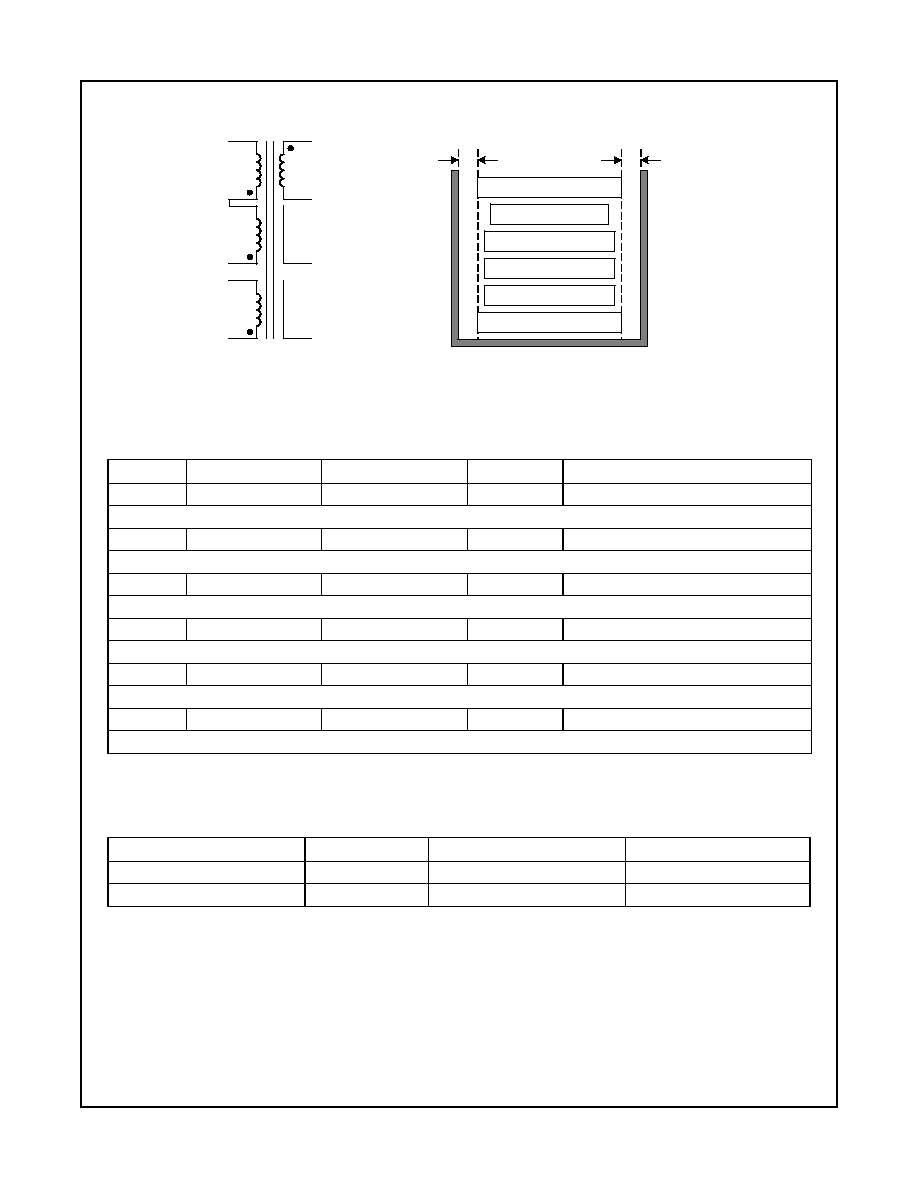
2. Inductor Schematic Diagram
Figure 27. Inductor Schematic Diagram
3. Winding Specification
4. Electrical Characteristics
5. Core & Bobbin
Core: EER2828
Bobbin: EER2828
Ae(mm
2
): 82.1
No
Pin (s
f)
Wire
Turns
Winding Method
Np1
3
2
0.3
× 2
31
Solenoid Winding
Insulation: Polyester Tape t = 0.03mm, 2 Layers
Shield
5
Copper Tape
0.9
Not Shorted
Insulation: Polyester Tape t = 0.03mm, 2 Layers
Ns
12
9
0.65
× 3
10
Solenoid Winding
Insulation: Polyester Tape t = 0.03mm, 2 Layers
Shield
5
Copper Tape
0.9
Not Shorted
Insulation: Polyester Tape t = 0.03mm, 2 Layers
N
Vcc
6
5
0.2
× 1
10
Solenoid Winding
Insulation: Polyester Tape t = 0.03mm, 2 Layers
Np2
2
1
0.3
× 2
31
Solenoid Winding
Outer Insulation: Polyester Tape t = 0.03mm, 2 Layers
Pin
Specification
Remarks
Inductance
1 - 3
607
H
100kHz, 1V
Inductance
1 - 3
15
H
9 - 12 shorted
Np1
5
6
1
2
12
9
3
N
Vcc
Ns
Np2
Shied
5
Shied
5
3mm
3mm
Ns
Np1
Np2
N
Vcc
Ns
Shield
Ns
Shield
14
www.fairchildsemi.com
FAN7602 Rev. 1.0.1
F
AN7602 Green Curren
t Mode PWM Controller
6. Demo Circuit Part List
Part
Value
Note
Part
Value
Note
Fuse
Capacitor
FUSE
1A/250V
C101
220nF/275V
Box Capacitor
NTC
C102
150nF/275V
Box Capacitor
RT101
5D-9
C103, C104
102/1kV
Ceramic
Resistor
C105
150
F/400V
Electrolytic
R102,
R112
10M
1/4W
C106
103/630V
Film
R103
56k
1/2W
C107
271
Ceramic
R104
150
1/4W
C108
103
Ceramic
R105
1k
1/4W
C109
22
F/25V
Electrolytic
R106
0.5
1/2W
C110
473
Ceramic
R107
56k
1/4W
C201, C202
1000
F/25V
Electrolytic
R108
10k
1/4W
C203
102
Ceramic
R109
0
1/4W
C204
102
Ceramic
R110
1k
1/4W
C222
222/1kV
Ceramic
R111
6k
1/4W
MOSFET
R113
180k
1/4W
Q101
FQPF8N60C
Fairchild
R114
50k
1/4W
Diode
R201
1.5k
1/4W
D101, D102
UF4007
Fairchild
R202
1.2k
1/4W
D103
1N5819
Fairchild
R203
20k
1/4W
D202, D204
FYPF2010DN
Fairchild
R204
27k
1/4W
ZD101, ZD201
1N4744
Fairchild
R205
7k
1/4W
BD101
KBP06
Fairchild
R206
10
1/2W
TNR
R207
10k
1/4W
R101
471
470V
IC
Filter
IC101
FAN7602
Fairchild
LF101
23mH
0.8A
IC201
KA431
Fairchild
L201
10
H
4.2A
OP1, OP2
H11A817B
Fairchild
15
www.fairchildsemi.com
FAN7602 Rev. 1.0.1
F
AN7602 Green Curren
t Mode PWM Controller
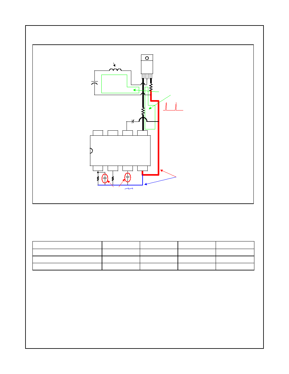
7. PCB Layout
Figure 28. PCB Layout Recommendations for FAN7602
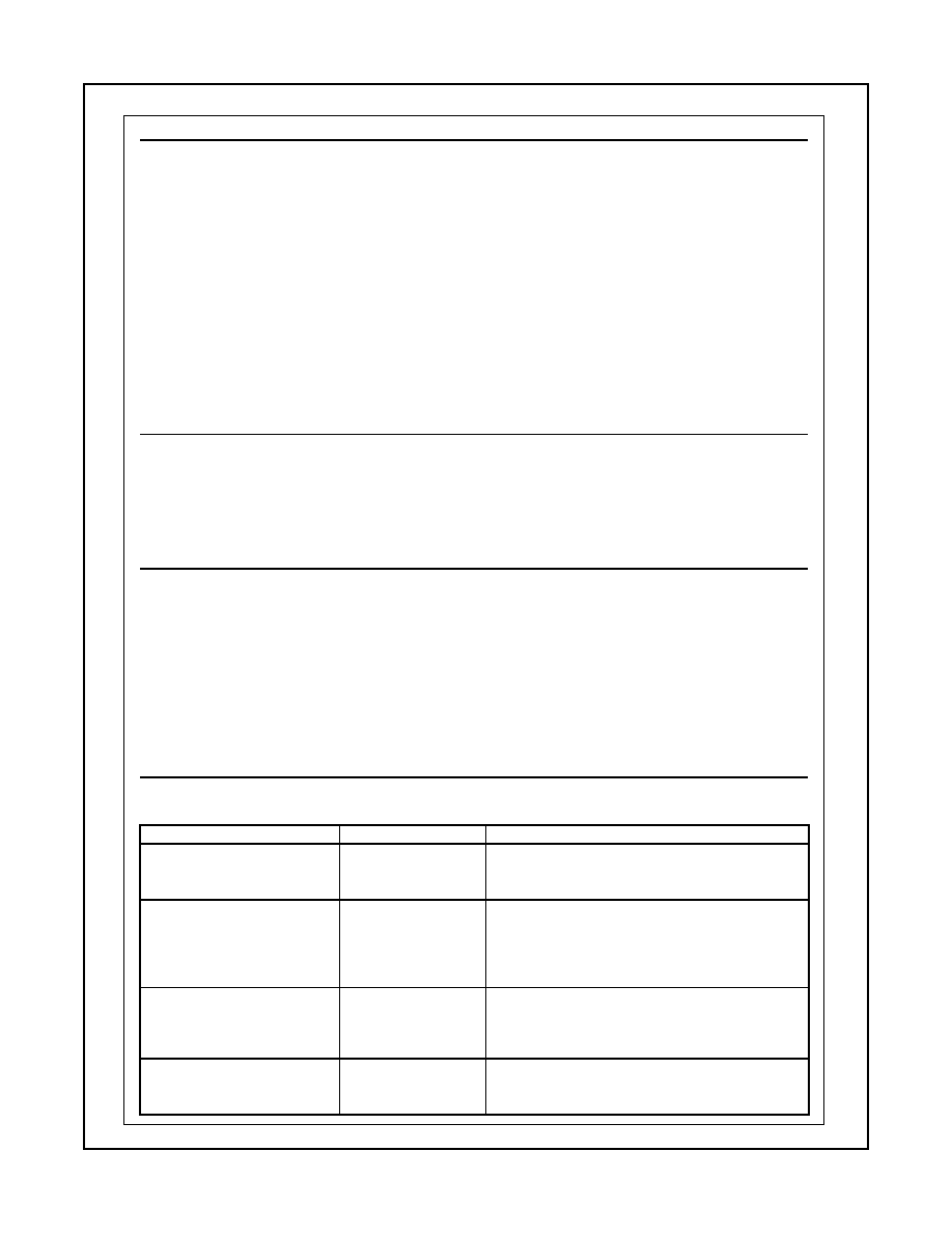
8. Performance Data
85Vac
110Vac
220Vac
265Vac
Input Power at No Load
105.4mW
119.8mW
184.7mW
205.5mW
Input Power at 0.5W Load
739.4mW
761.4mW
825.4mW
872.2mW
OLP Point
4.42A
4.66A
4.6A
4.4A
Minimize loop area
Separate power
and signal ground
Minimize leakage
inductance
F A N 7 6 0 2
1
2
6
5
8
7
YWW
3
4
Latch/
Plimit
GND
CS/FB
LUVP
Vstr
NC
Vcc
Out
Place these cap.
close to IC
DC
Link
Pulsating high current
Signal level low current
16
www.fairchildsemi.com
FAN7602 Rev. 1.0.1
F
AN7602 Green Curren
t Mode PWM Controller
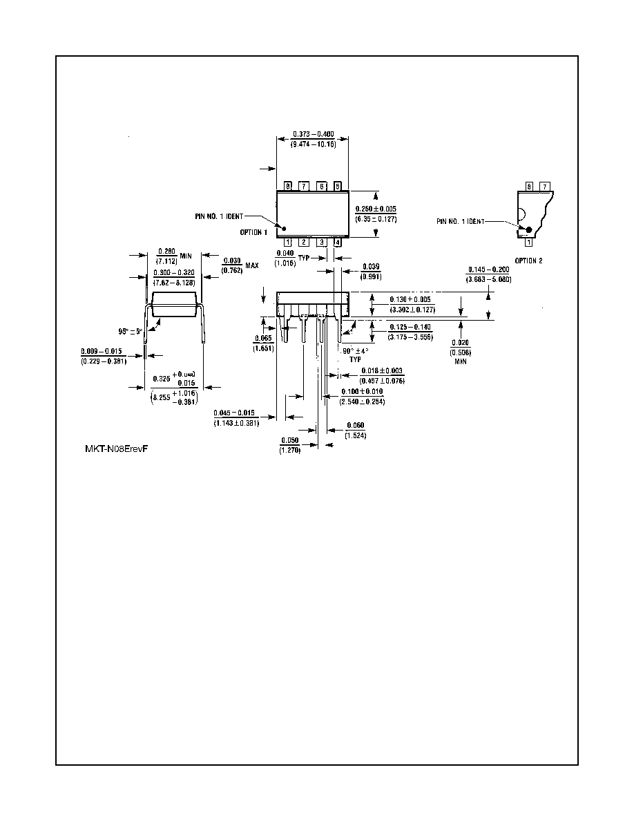
Mechanical Dimensions
Package
Dimensions in inch (millimeters)
17
www.fairchildsemi.com
FAN7602 Rev. 1.0.1
F
AN7602 Green Curren
t Mode PWM Controller
Rev. I19
TRADEMARKS
The following are registered and unregistered trademarks Fairchild Semiconductor owns or is authorized to use and is not
intended to be an exhaustive list of all such trademarks.
DISCLAIMER
FAIRCHILD SEMICONDUCTOR RESERVES THE RIGHT TO MAKE CHANGES WITHOUT FURTHER NOTICE TO ANY
PRODUCTS HEREIN TO IMPROVE RELIABILITY, FUNCTION OR DESIGN. FAIRCHILD DOES NOT ASSUME ANY
LIABILITY ARISING OUT OF THE APPLICATION OR USE OF ANY PRODUCT OR CIRCUIT DESCRIBED HEREIN;
NEITHER DOES IT CONVEY ANY LICENSE UNDER ITS PATENT RIGHTS, NOR THE RIGHTS OF OTHERS. THESE
SPECIFICATIONS DO NOT EXPAND THE TERMS OF FAIRCHILD'S WORLDWIDE TERMS AND CONDITIONS,
SPECIFICALLY THE WARRANTY THEREIN, WHICH COVERS THESE PRODUCTS.
LIFE SUPPORT POLICY
FAIRCHILD'S PRODUCTS ARE NOT AUTHORIZED FOR USE AS CRITICAL COMPONENTS IN LIFE SUPPORT
DEVICES OR SYSTEMS WITHOUT THE EXPRESS WRITTEN APPROVAL OF FAIRCHILD SEMICONDUCTOR
CORPORATION.
As used herein:
1. Life support devices or systems are devices or systems
which, (a) are intended for surgical implant into the body,
or (b) support or sustain life, or (c) whose failure to perform
when properly used in accordance with instructions for use
provided in the labeling, can be reasonably expected to
result in significant injury to the user.
2. A critical component is any component of a life support
device or system whose failure to perform can be
reasonably expected to cause the failure of the life support
device or system, or to affect its safety or effectiveness.
PRODUCT STATUS DEFINITIONS
Definition of Terms
ACExTM
ActiveArrayTM
BottomlessTM
Build it NowTM
CoolFETTM
CROSSVOLT
TM
DOMETM
EcoSPARKTM
E
2
CMOSTM
EnSignaTM
FACTTM
FAST
®
FASTrTM
FPSTM
FRFETTM
GlobalOptoisolatorTM
GTOTM
HiSeCTM
I
2
CTM
i-Lo
TM
ImpliedDisconnectTM
IntelliMAXTM
ISOPLANARTM
LittleFETTM
MICROCOUPLERTM
MicroFETTM
MicroPakTM
MICROWIRETM
MSXTM
MSXProTM
OCXTM
OCXProTM
OPTOLOGIC
®
OPTOPLANARTM
PACMANTM
POPTM
Power247TM
PowerEdgeTM
PowerSaverTM
PowerTrench
®
QFET
®
QSTM
QT OptoelectronicsTM
Quiet SeriesTM
RapidConfigureTM
RapidConnectTM
SerDesTM
ScalarPumpTM
SILENT SWITCHER
®
SMART STARTTM
SPMTM
StealthTM
SuperFETTM
SuperSOTTM-3
SuperSOTTM-6
SuperSOTTM-8
SyncFETTM
TCMTM
TinyLogic
®
TINYOPTOTM
TruTranslationTM
UHCTM
UniFETTM
UltraFET
®
VCXTM
WireTM
FACT Quiet SeriesTM
Across the board. Around the world.TM
The Power Franchise
®
Programmable Active DroopTM
Datasheet Identification
Product Status
Definition
Advance Information
Formative or In
Design
This datasheet contains the design specifications for
product development. Specifications may change in
any manner without notice.
Preliminary
First Production
This datasheet contains preliminary data, and
supplementary data will be published at a later date.
Fairchild Semiconductor reserves the right to make
changes at any time without notice in order to improve
design.
No Identification Needed
Full Production
This datasheet contains final specifications. Fairchild
Semiconductor reserves the right to make changes at
any time without notice in order to improve design.
Obsolete
Not In Production
This datasheet contains specifications on a product
that has been discontinued by Fairchild semiconductor.
The datasheet is printed for reference information only.